Blinken Hex Lights —
Time to upgrade some of my binary Blinkenlights plug-ins to 7-segment LED hexadecimal versions.
In the design of my Hol-1 8-bit CPU I have been leaving rows of pin headers for the attachment of LED indicators. Mainly because you can never have enough Blinkenlights twinkling on a homebrew computer but also because they have their uses for debugging, signal injection and one day they could be used to connect to a control panel.
However, since the creation of the Hol-1 Memory Management Unit I have found the binary Blinkenlights a pain to use. Programming in 1’s and 0’s may be a geeky achievement but it is also tedious and error prone. To improve this situation I need to replace the MMU binary plug-ins for memory addresses and memory contents with hexadecimal alternatives

Here you can see the binary and hexadecimal plugins in operation. From the top and going clockwise these four circuit boards are the Hol-1 Registers, the Hol-1 ALU, Hol-1 RAM and the Hol-1 MMU complete with two Blinken Hex Light displays.
Blinken Hex Light Design
The binary Blinkenlights plugged into a straight row of 9 male header pins. Straight so they could cut across 8-bit data bus traces and the 9th was required to provide a ground connection for the plug-in’s LEDs. This means the binary plugins are feeding off the positive signals on their data buses to light their corresponding LEDs. Not ideal for signal strength but the plug-ins needed to be small and the Hol-1 design has a very low fan-out from any TTL output so an LED’s drain on the signal voltage was not a problem. They’re also plug-ins, so if there was a problem with signal strength or overall power consumption they can be unplugged without impacting CPU function.
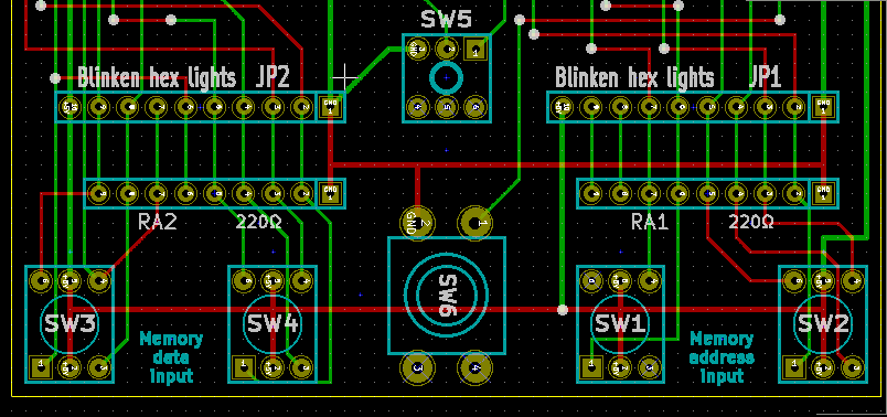
Replacing the 8 binary LEDs with a dual 7-segment LED display (that’s 16 LEDs and a couple of decoding chips) would be too large a drain on signal strength though so a 10th male header pin would be required on the MMU circuit board to provide separate power to the plug-in. I had already considered this in the Memory Management Unit design though and provided 10-pin rows for displaying memory address and the value to be programmed into memory. Looking at the MMU PCB layout below the 10-pin male headers for the Blinken Hex plug-ins from left to right are [+5V pin][8 data pins][Ground pin]. The 220R resistor arrays shown below each Blinken Hex plugin are not actually necessary for this hex plug-in design or the later version of the binary plug-in (as they contain their own current limiting resistors) but are needed if older binary plug-ins are used else the LEDs will blow. These plug-ins are therefore interchangeable and backwardly compatible if the binary plugins are connected to just the 8 data pins and the ground pin. I shall have to mark the ground end of each plug-in with a dab of coloured nail polish (when the wife’s not looking) although there is no danger should they be plugged in backwards.
Fortunately I had the foresight to leave some space around these male header pins for a larger plug-in and ensured that only low profile components were used nearby. But with hindsight I would move the plug-in headers a row or two higher to give more space around the rotary switches. I should also retire my older binary plug-ins and remove the need to add resistor arrays but they are so fiddly and time-consuming to make that I still don’t have enough of the newer model.
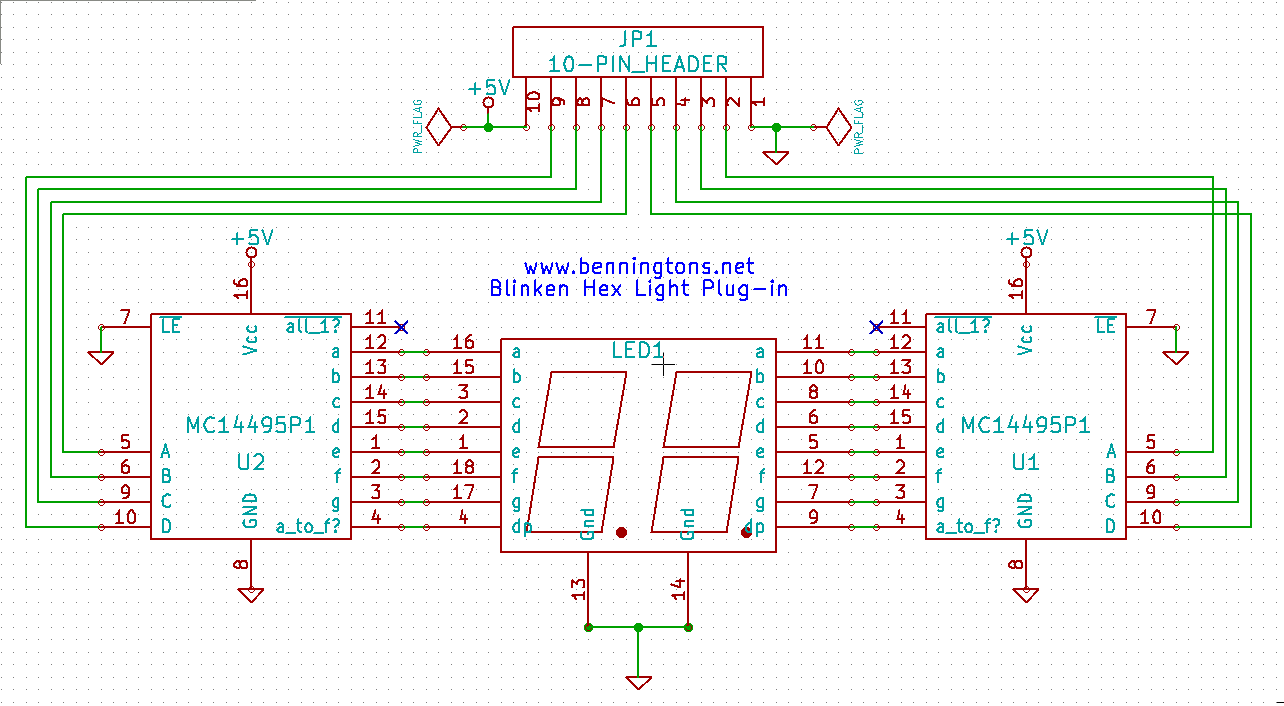
Looking at the below schematic for the Blinken Hex plug-in you’ll see that they’re quite simple. At the top is the 10-pin female header for connecting to the MMU and two MC14495P1 chips are then used to decode the 8 binary inputs into hex outputs that directly drive a dual 7-segment LED display.
My original design was based on some Fairchild DM9368 7-segment decoder chips which I purchased from China. I was feeling fortunate to find a supplier of these discontinued IC’s and waited ages for delivery only to find they were fakes (they would display digits 0-9 but blank outputs instead of A-F). I wasn’t put off by this experience though (or rather I didn’t learn from it!) and next ordered some equally discontinued Motorola MC14495P1’s from China and this time was fortunate to get the real thing (or maybe some out of spec seconds but they’re working fine for me).
The MC14495 is a CMOS IC that works fine with the TTL voltage range. The datasheet is quite straightforward for inputs and outputs but I’ll explain some of the ancillary pins.
Latch Enable (pin 7) is kept low to enable all input data to be directly output to the 7-segment display. If held high then inputs would be ignored and the output would remain fixed (latched) to the last enabled input.
Output all_1 (pin 11 and called output j in the datasheet) would be low whenever all inputs are set high. I have no need for this in this plug-in so the pin is not used.
Output a_to_f (pin 4 and called h+i in the datasheet) is high whenever the output is in the a to f range. As the output for the digit b is similar to the output for the digit 6 I have used this a_to_f output to drive the decimal point on each 7-segment display. I can therefore easily see if a digit above the usual decimal range is displayed and hopefully make fewer mistakes when programming Hol-1.
The dual 0.56″ 7-segment display used needs to be a common cathode version for compatibility with the MC14495 outputs, mine are marked as E20561. For construction purposes the longer the component pins the easier they’ll be to solder, as we’ll see next.
Blinken Hex Light Construction
I should start by saying this is very fiddly for through hole construction and given that the design is based on a discontinued IC then I would encourage you to consider an alternative. Maybe a female header to 10-way ribbon cable to a control panel that uses an alternative chipset? I’ve persevered with this approach because I wanted the plug-ins to be in keeping with the rest of Hol-1. i.e. of a similar era and construction style. Had the plug-ins been bespoke multi-sided PCBs with surface mount components and maybe a small microprocessor to drive the LED outputs then it would look suspiciously like the plug-ins were driving Hol-1 rather than vice-versa.
Each plug-in is based on a 9 x 10 grid of double-sided perfboard (2cm x 2.5cm or 7/8″ x 1″) and requires wiring connections between 60 of those 90 holes.
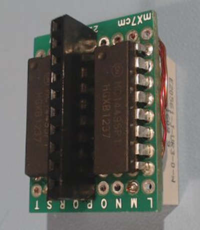
The row of 10 female header pins and two ICs are on the bottom of the circuit board and the dual 7-segment display on the top. As the display module will cover all but one row of each IC the order of construction is key.
First solder all trace wires between the header pins and their IC sockets. I found using fine wine and placing each stripped end between pin and plated through hole was the quickest and neatest way to go. I then tried two methods for making connections to the 7-segment display pins.
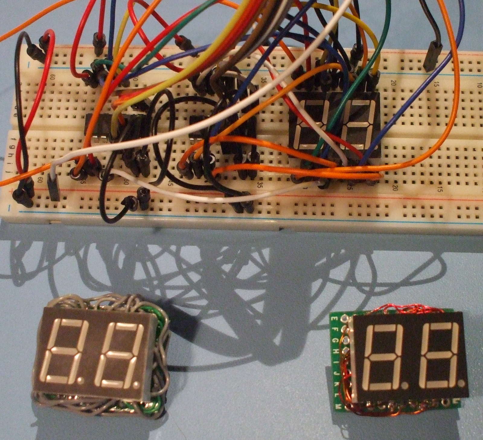
The first was to solder longer than needed leads to each IC output pin. Then insert the display module and solder the 18 loose ends of each lead to the required module pin, testing the continuity of each to ensure the right connections are made. This method (with a small soldering iron tip) works and if there are any problems they’re generally fixable but the result is a messy birds nest around the plug-in.
The next method was to use fine gauge enamel coated copper wire salvaged from a transformer in an old mobile phone charger. One end of each wire was again soldered to each IC output pin but then cut and shaped to reach the required through hole for the display module. Inserting the end of each lead into the required hole but not yet soldering them. A dab of glue was used to hold some wires in place. The result was 18 wires hopefully staying in the right holes whilst the display module pins were inserted to wedge them in place. Careful inspection was then required before they were then soldered. This method produced a neater looking plug-in but if there were any mistakes then it would be hard to correct or even recover components. Fortunately all was ok.
Above is the original breadboarded plug-in, the birds nest version on the bottom left and the final neater version on the right.
TTL Logic Testing
The binary and hex Blinkenlight plugins are usually sufficient for debugging during the construction of my 8-bit CPU, especially as the clock speed can be slowed or even halted and progressed one step at a time. They’re not the only logic testing tools I have been using though.
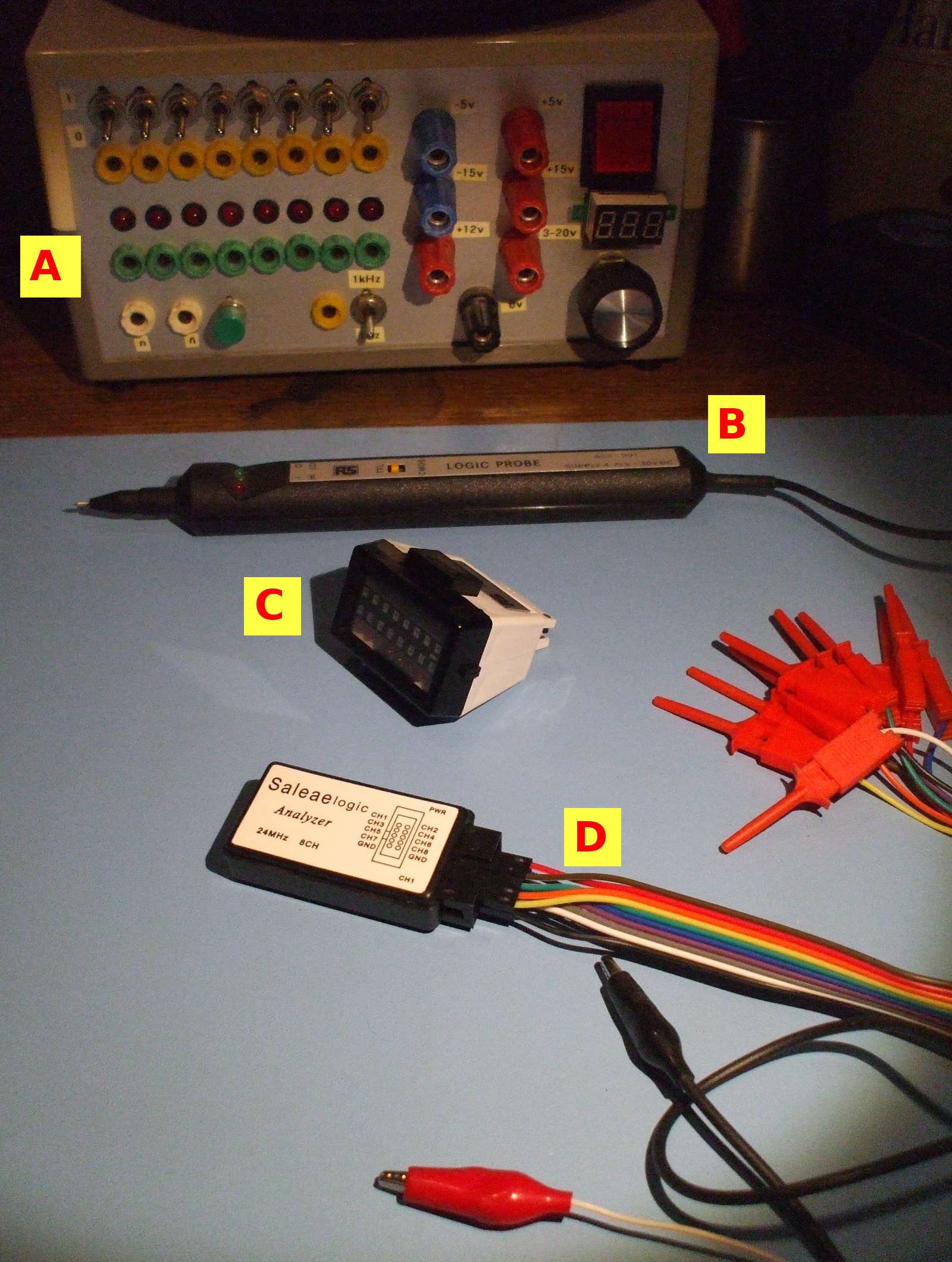
In addition to a multi-meter to test power supply and an oscilloscope to check data waveforms and frequencies I find the above useful.
A. my homemade Minilab has a row of green banana plug sockets connected to LEDs to indicate logic levels. Test leads can therefore be connected to any part of Hol-1 to check logic levels.
B. a standard Logic Probe has a rear cable leading to two crocodile clips (bottom of photo) which are connected to the 5V supply and ground. The tip of the probe can then be used to test logic levels at any point on Hol-1. My Logic Probe is a common UK variety badged as RS 653-991.
C. is a rarely seen and ingenious TTL Logic Checker. It can be adjusted for 14 and 16 pin ICs and simply clips over the top of any TTL IC. It determines power and ground supplies and displays logic levels via two rows of red LEDs on top of the unit. It can be frustratingly fiddly to get it properly clipped onto an IC but once in place it is fascinating to use. Mine is badged as RS 423-920.
D. is a cheap imitation of a Saleae Logic Analyser connected to the red test clips on the right of the photo. I’ve not needed to use this on Hol-1 yet because a very slow clock speed can be used and all the above testers will flash slowly to indicate changing logic levels. But once Hol-1 is complete and I start to test at higher clock speeds then all the previous logic testers will be of little use. This is when I shall rely on this Logic Analyser to decipher what’s happening at a bit by bit level within Hol-1. The Analyser connects to a PC via USB and (being a devout Linux user) I use PulseView from the Sigrok project to display and analyse the output (also available for other OS’s).
As each circuit board of Hol-1 is completed I go to the trouble of producing a spreadsheet showing the expected state of every pin of every IC. This is a big help when re-visiting previous boards to check that they’re working correctly. It’s a tedious process but a time-saver in the long-run.
Well those Blinken Hex Lights make the Hol-1 MMU easier to program. It’s about time I completed this 8-bit CPU.
Categorised as: Electronic Stuff | Homebrew 8-Bit CPU
Comments are disabled on this post