8-Bit CPU – ALU —
Building an Arithmetic & Logic Unit (ALU) with TTL logic.
Recap:
My quest to build an 8-bit central processing unit (CPU) from transistor transistor logic chips (TTL) continues. This initial venture into CPU design being very much guided by Ben Eater’s video tutorials for a computer built on breadboards. Please refer to Ben’s videos for a thorough explanation of how a computer works. I shall instead focus on my design modifications and a more permanent project build using circuit boards.
Having completed modules for the CPU’s registers and to generate a clock signal my next step is the ALU. As the name suggests the ALU provides the arithmetic and logic functions for the CPU. Although this particular basic design only provides addition, subtraction (actually just addition again but with the 2nd operand negated) and no bitwise logic functions, so I’ve added some status checks to enable programs to have some logic.
Initial design:
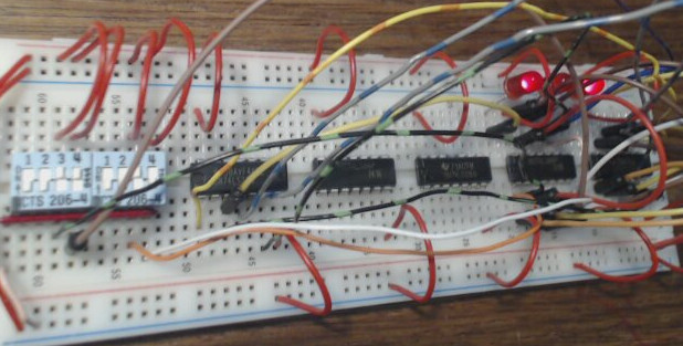
At the core of this ALU are two 4-bit adders (74LS283’s) with the carry-out of one fed to the carry-in of the other to create an 8-bit adder. In this first photo I’m using two 4-bit DIP switches to test the first of these adders, selecting the numbers 3 and 2, which result in a binary 5 displayed on the three test LEDs. So that’s addition sorted and repeated additions could be used to provide multiplication.
Both A and B registers are directly wired into the ALU, so only those registers can be added together. The result is fed to a 74LS245 bus transceiver which would usually be called the accumulator (A) but I’ve been referring to it as the sum, or S, register to avoid confusion with register A. But the S register is not really a complete register because it can’t retain any values independent of the A and B registers. i.e. whenever A or B change values then S will automatically change to reflect the sum of the two. No specific command is required to perform the addition, simply loading A or B with a new value will change S. But, as with the other registers, the S register does have a control line that is used to output its contents onto the data bus when the control line (called sum-out) is low.
To provide a subtraction function, eight XOR gates (provided by two 74LS86’s) are used to generate a 1’s complement (converting 1’s to 0’s and vice versa) of the value in the B register by XOR’ing each bit of the B register with a 1. That 1 is provided by a control line that is held low for addition and high for subtraction. That control line is also used to add 1 to the generated 1’s complement value (via the carry-in pin of the lower half adder) to create a 2’s complement value of the contents of register B (i.e. the value from register B is negated). Thus the value in register A is added to the negated value in register B and the result (i.e. A – B) is held in the S register. And so that’s subtraction and multiple subtractions could be used to provide a divide function, if checks on the resulting sum of each subtraction were possible.
I should add that the contents of the A and B registers remain unchanged when arithmetic is performed in the ALU. They just provide the two input values to each addition or subtraction.
Status flags:
This initial design provides basic arithmetic but no logic. I considered adding bitwise operations such as AND, OR or shift left/right commands but didn’t expect to use them on this simple 8-bit CPU. Of more use to the short programs that I hope to run on Hol-1 are checks on the sum register. Such checks could then be used to support IF statements and conditional loops and thus provide some logic.
Carry? – Was an obvious choice because the higher 4-bit 74LS283 adder provided an unused carry-out pin. By providing this to a Status & Control bus I could signal to other modules of this 8-bit CPU that the result of any addition had exceeded the upper limit of the signed 8-bit number range (-127 to 127). Future programs could use this to signal an error or maybe as an input to an upper 8-bit number (i.e. 8-bit CPUs can still cater for 16, 32, 64-bit or higher number ranges if each 8-bit portion of these larger numbers were processed in turn. Slow but possible.). For subtractions the carry flag is always on (high) until an underflow situation occurs, i.e. the result is less than -127. This could also be used to signal an error or to enable working with number ranges beyond the signed 8-bit range.
Odd/Even? – The lowest bit of the sum register can be used to feed an odd (high) or even (low) status flag. Such a flag isn’t commonly seen but could be of some use to programs and may even be used to signal a true or false status?… Convinced? Ok, I admit this flag was created by mistake! I intended to create a negative/positive flag by checking the upper bit in the S register but took a big-endian view of what is a little-endian CPU design. I got the neg/pos connection right when this circuit was on a breadboard but made the mistake when transferring to a soldered PCB. I could have easily corrected this but hey, an odd/even status flag may prove useful?
Negative/Positive? – This was the flag I intended to create! A feed from the upper bit of the sum register will enable programs to check if the result of an addition/subtraction was a negative (high) or a positive (low) number.
Zero? – Having used all the obvious feeds available to create status flags there was a key one missing. Knowing if the sum register was positive or negative when performing a subtraction would enable programs to test if the value in the A register was greater or less than the value in the B register. But how do you test if the A and B registers contained equal values? This wasn’t possible on the initial ALU design so I added eight diodes to feed all of the eight bits of the sum register into one “zero (low) not-zero (high)” status flag. In doing so I also needed to add a pull-down resistor to ensure that the zero flag really was low when no signals were being received through the diodes from the sum register. Instead of diodes I could have used an 8-input OR gate, an octal buffer with the outputs combined or various combinations of logic chips to provide a TTL solution for a zero flag but I instead applied my principles of ‘using whatever components I had available’ and ‘making best use of circuit board space’.
Control flags:
With a total of four status flags to feed to other modules on this CPU I decided to combine these with up to four control flags and make use of an 8-way ribbon cable connection. These control flags are:-
Sum-out – To be set low to output the contents of the S register onto the data bus. It’s worth noting that all status flag checks are made on the inputs to the 74LS245 bus transceiver and not the outputs. Often programs will need to know if the A register is greater than, less than or equal to the B register but have no need to store the result of the arithmetic involved.
Add/Subtract – Set low and the ALU will perform additions with the values in the A and B registers. Set high and the value in the B register will be subtracted from the value in the A register and the result placed in the S register.
That left two remaining status/control bus flags available for further functions. Considering the limited space remaining on the intended PCB for this ALU and the small and fairly simple programs that this CPU will be running I’ve only opted to use one of these remaining flags at this time.
Inc/Dec – One of the most frequently used arithmetic functions is to increment or decrement a counter by 1 (i.e. i++ or i−− in C). But I’ve already completed addition and subtraction circuits so you may wonder why I need to create an Inc/Dec control? Well to increment A, I would first need to save what’s in B to memory, load 1 into B, move the result of A+B into A and then recover the original contents of B from memory. That’s multiple clock cycles and I’ve brushed over the need to select the correct place in memory to store the contents of B. It’s also a long string of commands that will eat-up the available memory for storing a program, just to increment A.
My design adds a 74LS245 bus transceiver to the register B input so that an Inc/Dec control flag can be used to switch off the link to register B. This would leave the ALU inputs from register B floating so I’ve used pull-down resistors on all input lines except for the lowest bit which has a pull-up resistor. Thus setting the B input to 1. The state of the Add/Subtract control flag will then determine if an increment or decrement function is performed. Thus an INCA or DECA command would be possible without affecting register B or memory and will use minimal clock cycles and help to keep programs small.
Status/Control flags that got away:
Here are a few ALU alternatives that I’d like to add but will have to wait till my next CPU.
Bitwise logic – e.g. AND, OR and particularly the left/right shifting of a register and maybe the testing/setting of a specific bit in a register.
Multiply/Divide – all possible with some looped additions or subtractions, helped further with bit shifting. Nice to have as specific functions but I see that even the 74181 ALU (which I intend to use in HOL-2) doesn’t provide them.
Static values – I’ve already provided a 1 via the Inc/Dec control and this can be turned into a -1. I believe some common static values can help to reduce the need for such values being incorporated within programs. i.e. the ability to zero any register in a single clock cycle would be good but holding complex numbers such as pi is beyond my 8-bit dreams.
Register selection – Fixing the ALU to work with only the A and B registers is restrictive. More so when A-B is possible but not B-A. Selecting the incoming registers and their order would be very useful.
Construction:
Breadboard construction was initially ok when testing each chip but soon got messy.

So here is my design for a soldered perfboard layout (click on the image to get a bigger picture). I tend to refer to these as PCBs but there are no tracks on the board. All connections are made by soldering wires to each pin of each component.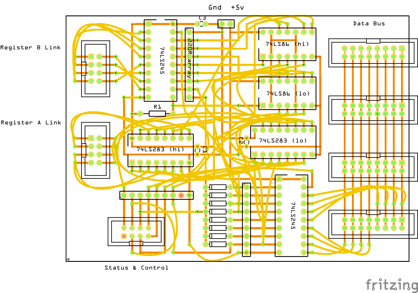
I have used the same 8cm x 12cm double-sided perfboard as I used for the CPU’s registers. These provide a 29 x 41 grid of holes which was more than ample for my six chip ALU design. In fact, without overly compressing the layout, I was still left with a 10 x 41 strip of holes on the right of the board. I considered adding more ALU functionality but eventually opted to use this space for the hub of the data bus. A line of connected ribbon cable sockets that will connect the data buses from multiple boards together into one data bus. I originally intended to use a strip of veroboard for this hub and would have liked to have kept it as a separate module in its own right but using this available space on the ALU seemed right. You’ll notice that for single board to board links I have used 8-way ribbon cable but for the data bus I have used 16-way to make a hub of parallel connected cables possible.
Along with the logic chips, diodes, ribbon cable connectors and pull-up/down resistors (using a single-in-line SIL array to save space) I have also added a couple of 9-pin blinkenlight connections and a scattering of powerline capacitors. As with the CPU register board these capacitors are intended to provide a quick source of power to assist the fast operation of the logic chips. Just how fast the board will go and just how many capacitors are needed I really don’t know but I could add more or increase their value in the future, if really necessary.
Wiring on the board appears more complex than the register board but that is largely due to the data pins of most of the IC’s used not being in a neat A0 to A7 order. Instead they appear on both sides of each adder and XOR chip which results in a spaghetti wiring plan. I’ve continued to use enameled copper wire for the data lines and different coloured wires for each status and control line.
Testing involved the use of a breadboard with all control lines from both the register and ALU boards connected to it by jumper leads. These could then be set to high or low to control both boards and test each ALU function. Blinkenlight plugins on both boards displayed A, B and C register content, data bus values, status & control flags and the contents of the ‘S’um register. Connecting the clock signal generator enabled testing of repetitive arithmetic, such as the increment and decrement features. With the exception of one dry joint all soldered connections tested ok and I’m glad that I haven’t managed to reverse the pin order on any of the buses!
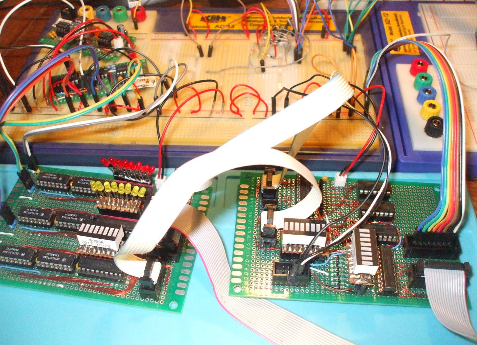
Here is the completed ALU board on the right with the registers board on the left and the clock modules and test control breadboard in the background. I really must practice at taking better photos! You may notice that I’ve only soldered two of the intended four ribbon cable connectors to form the data bus hub on the right of the ALU board. This is partly because the others are not needed yet and partly to reserve some space on the board in case I need to make any late modifications to the completed CPU.
Parts List:

80x120mm double-sided prototype PCB (a.k.a. perfboard)
C1-3	Ceramic Capacitor 100nF
IC1-2	74LS283 4-bit binary full adders (with carry)
IC3-4	74LS86 quad 2-input XOR gates
IC5-6	74LS245 8-bit bus transceiver, non-inverting, tristate (i.e. on, off and disconnected)
6 x		14, 16 and 20-pin IC sockets for the above ICs
1 x		JST PH 2-pin male connector (for power supply - I prefer a click & hold socket for these)
1 x		220R single-in-line (SIL) resistor array (for pull-down)
1 x		47kR resistor (for pull-up)
8 x		small signal diodes (believed to be 1N1418 or similar)
4 x		16-pin (2 rows of 8) male IDC box headers (for ribbon cable bus connections)
3 x		8-pin (2 rows of 4) male IDC box headers (for ribbon cable direct link connections)
and various bits of wire and enamel coated copper from scraps.
Most of the above were from odds and ends that I already had, but to give an indication of the cost of this ALU, all the above could be purchased for less than £4 ($5). I usually purchase from China via Aliexpress which take between 2 to 5 weeks to deliver to the UK. Thanks to their low prices I always purchase more than I need to build up stock for future builds and experiments. If I’m feeling impatient then I’ll pay more for a quick delivery from Rapid Online in the UK.
That’s the Arithmetic & Logic Unit completed for my “Hol-1” 8-bit CPU. Next the Random Access Memory (RAM).
Categorised as: Homebrew 8-Bit CPU
Comments are disabled on this post