Sequential Logic Tutor —
Following on from the Combinational Logic Tutor this next item is on the next rung up the computing evolutionary ladder. To explain I’d better start with combinational vs sequential logic theory.
Combinational and Sequential Logic
As seen in my previous post, connect the different logic gates and the Combinational Logic Tutor’s output is generally* a direct result of whatever the input switches are currently set to. Change the inputs and the output will change immediately. If you know the logic algorithm and the 1’s and 0’s currently set as inputs then you can predict what the outputs will be.
Sequential logic follows all the same logic rules but it is enhanced by having some memory of previous inputs. To predict what the outputs will be you would need to know the history of sequential inputs since the unit had been powered on.
Combinational logic can add numbers together but all numbers have to be presented as inputs at the same time. The more numbers the larger and more complex the logic algorithm required.
Sequential logic can add an endless list of numbers and because one number could be input at a time then the logic algorithm is much smaller, although with the added complication of memory.
*I have generalised here to show the intended difference between the combinational and sequential logic tutors. It is actually possible to use the Combinational Logic Tutor to create various types of memory devices i.e. latches and flip-flops.
In the software world I would describe combinational logic as being stateless or as having no context. e.g. a simple web-server could often be stateless because the output is a direct result of whatever URL and data was input from the client.
To have state or context the server would need to remember what that particular client had previously been doing, thus applying sequential logic. e.g. in a more complex web-server the output may be dependent on knowing if the client had already logged on correctly or what items may be in the client’s shopping basket.
So, at a simple logic level we can expect a Sequential Logic Tutor to contain some form of memory and probably some form of clock to synchronise the sequencing of inputs. i.e. you’ll need some time to setup the inputs without the Tutor prematurely acting upon what you have changed so far. So a clock signal is used to notify the Tutor that you’ve finished changing the inputs so it can read in the next number or instruction.
COMPUKIT Sequential Logic Tutor
This device has many similarities with the Combinational Logic Tutor so I shall try not to repeat myself. I acquired both Logic Tutors a few years ago following a surplus sale at a UK technical college. I paid £7.50 for the Combinational Tutor and only £5 for this Sequential Tutor.
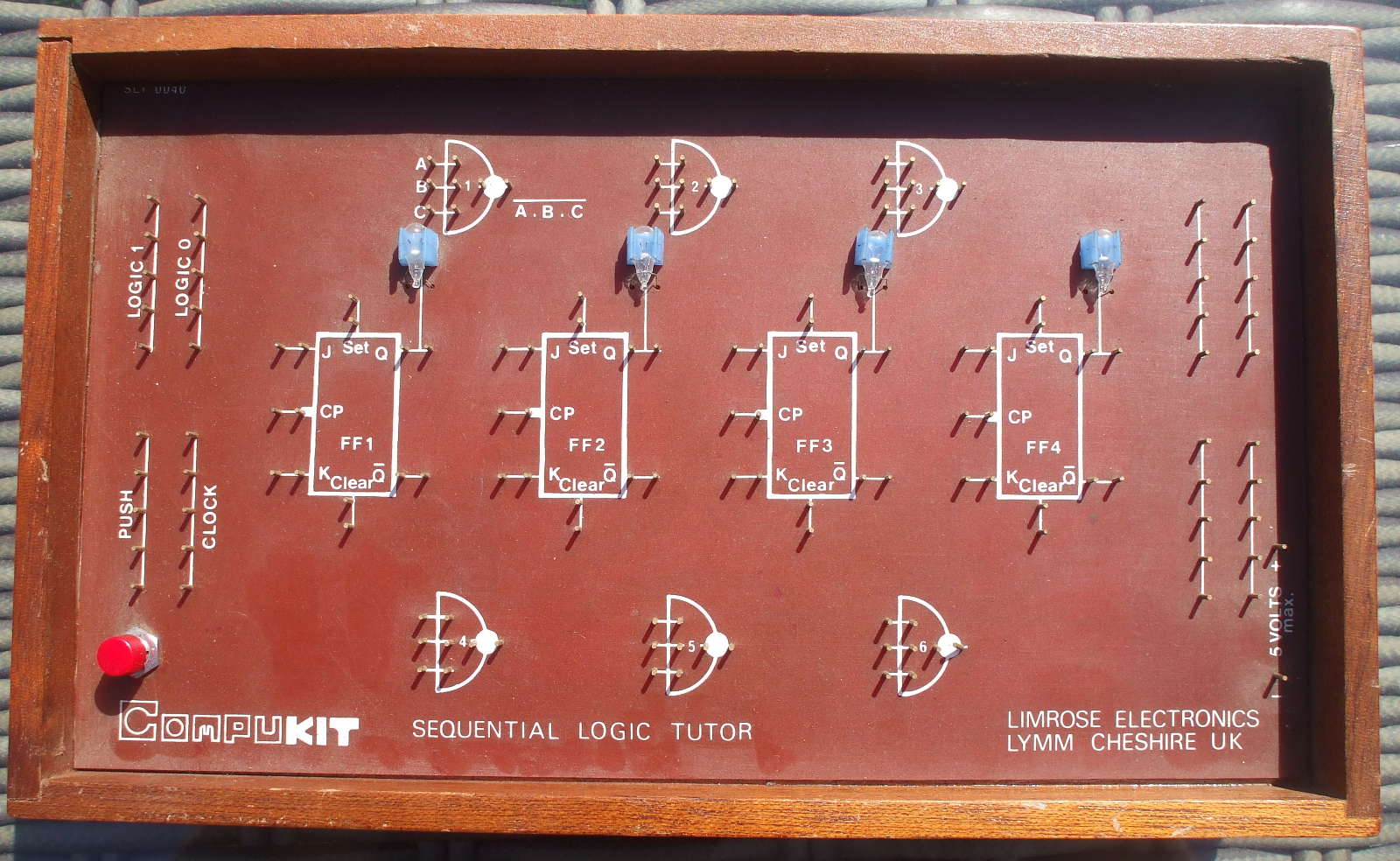
The Sequential Logic Tutor also has logic symbols printed on its front panel and pins on all inputs and outputs to enable them to be connected by jumper wires. The variety of logic gates is reduced to just NANDs but in the centre of the front panel are four flip-flops. A flip-flop is a basic memory unit that can remember 1 bit (0 or 1). So this Logic Tutor has 4-bits of memory.
In total the unit offers:
6 x 3-input NAND gates across the top and bottom
4 x flip-flops across the middle
4 x indicator lamps already wired to each flip-flop output
1 x momentary push button in the bottom left alongside 5 pins labeled PUSH and 5 labeled CLOCK
5 x pins labeled LOGIC 1 and 5 x pins labeled LOGIC 0 on the left hand side
4 x sets of 5 connected pins on the right hand side
2 x power supply pins in the bottom right labelled 5 VOLTS max. With better spacing to the + and – pin labels than the combinational tutor had.
At this stage I’m not actually sure what kind of flip-flop is displayed? The outputs are clearly Q and Q but there are inputs for Set and Clear (suggesting a simple Set-Reset latch), an input called CP (suggesting clock pulse or Enable, making it a gated SR latch) and also inputs labelled J and K (suggesting it’s a JK flip-flop).
The actions of Set and Clear on the 1-bit of memory are obvious and CP (or Enable) is used to disable or enable the Set and Clear actions.
But in a JK flip-flop the J and K replace the need for Set and Clear. J=Set, K=Clear and if they’re both set then the contents of the memory is inverted or flipped (hence the name flip-flop), which is something an SR latch cannot do.
Whether these flip-flops are capable of being SR latches or JK flip-flops or a combination of both will be revealed when I open it up.
Research
This ‘Compukit’ Sequential Logic Tutor is also made by Limrose Electronics and it has the product number SLT0040 printed in the top left. An SLT0040P5 with an identical layout but in blue and with a mains supply to 5V power supply is still listed on their website for £180.
The modern version has a ‘clean manual pulser’ so it will be interesting to see if my vintage version has any switch de-bouncing. Judging by the type of sprung switch used I suspect it relies upon a quick mechanical make & break connection.
Just in case these units don’t prove to be ‘student proof’, Limrose also provide spare switches, voltage regulators and LEDs (an upgrade on the old style lamps used in my logic tutors). They also provide packs of patch leads, which are the sort of thing that’s bound to go missing as I have had to make my own.
A 1973 advert for this Sequential Logic Tutor in Wireless World – ‘teaching logically made easy…’ prices the SLT0040 at £28.
Otherwise there is nothing more to be found about this tutor on the Internet.
External Inspection
As with the combinational tutor, this unit is slightly smaller than A4 paper size, in a nice hardwood case with a plywood back and a front panel that I now know to be the reverse of a PCB (probably fibreglass).
The unit is dirty, the wooden case has some scratches but the white lettering on the front panel is in good condition – and this time without any pencil marks.
The same recessed toggle switch for power is on the right hand side and this time it has a metal label showing which way for on/off. This also reminds me that this unit will have a battery that I will need to remove to avoid any potential damage from leakage. The battery’s presence is also confirmed by the weight of the unit.
Other than a bent pin on one of the NAND gates the unit is physically ok other than the rear panel. Unlike the previous tutor this rear panel is flush with the base of the unit and the brass screws are not countersunk. In fact several are fitted at angles meaning this unit could easily scratch your desk or table top.
Internal Inspection
Removing the 6 x brass screws allows the plywood back to be removed to reveal another Ever Ready 126 4.5V battery shielded from the circuit board by a sheet of polystyrene. This time the battery is securely in place and also wired to the power switch and circuit board.
The battery has more leakage stains than the one removed from the combinational tutor but is still a keeper. You just don’t see this type of battery anymore so I shall attempt to clean them up and replace their zinc-carbon cells.
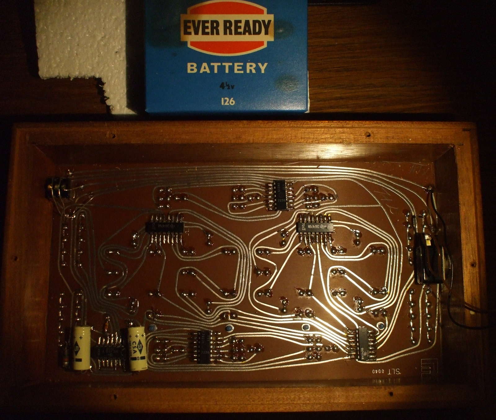
Inspecting the circuit board reveals no cracks or obvious damage other than a loose wire from the power switch. So the Tutor wouldn’t have worked from the internal battery and would have required an external supply.
In addition to the 74 family logic chips there are also a few passive components. Here is the bill of materials:
7400 – Quad 2-input NAND gate (Sescosem)
SN7404N – Hex inverter (by Texas Instruments)
2 x 7410N – Triple 3-input NAND gates (ITT)
2 x SN7476N – dual J-K flip-flop (Texas Instruments)
2 x 100uF electrolytic capacitors
2 x small signal diodes
1k resistor
SPST toggle switch for power
SPDT push button switch for logic pulses
IC date codes range from the 20th to the 44th week of 1972 suggesting this unit was probably constructed in late 1972.
The general layout of these logic tutors is to have the IC’s directly wired to pins on the front panel. They have no internal circuitry of interest other than power distribution but in this case we do have some passives and a 7400 setup to provide a clock signal.

This is a gated SR latch with the capacitors providing a delay to the perpetual set/reset motion of the circuit and the NAND output providing a TTL square wave clock signal. Whilst the gated SR latch is text book I find the use of the capacitors and diodes to generate a continuous clock signal both simple and effective.
This clock generates a 4.7Hz signal with a 50% duty cycle (half the time on and half the time off). Reducing the 100uF capacitors would increase the clock speed and vice versa. As a rough rule of thumb the sum of the two capacitors in micro-Farads should give the clock’s time period in milli-seconds.
Now we know the chipset for this logic tutor then the function of the (pre)set, clear, J, K and CP inputs is explained by the function table in the 7476 datasheet.
Restoration
Well there’s nothing really required. I straightened one pin, used a dry paint brush to clean dust from the front panel and insulated the disconnected battery leads.
Fitting the rear panel properly and ensuring the screws went in straight sorted the problem with them protruding.
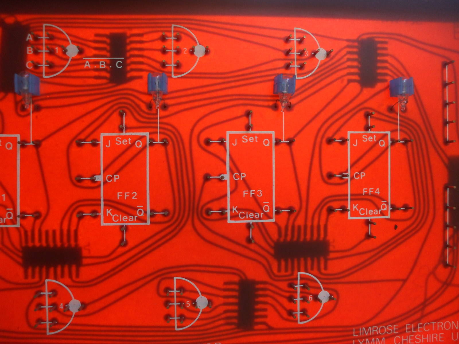
Here’s a shot of light shining through the circuit board to show both sides. Internally lit I find these tutors do have some artistic merit.
On power-up from a 5V supply all the bulbs lit fully. Using jumper wires I then created a sequential 4-bit counter to test each flip-flop by connecting the output of each to the J and CP input of the next. Connecting the J and CP inputs of the 1st flip-flop to the push button completed the circuit. Each press of the button was then counted across the 4 lamps.
Well that’s the Sequential Logic Tutor. A simple device from yesteryear that still works ok and is still a useful, hands-on educational tool.
Categorised as: Silicon Heaven
Comments are disabled on this post