Maplin Minilab —
Published in the September 1983 edition of “Electronics, The Maplin Magazine” the Minilab didn’t even get a mention on the front cover but this DIY power supply with extras for the electronics experimenter was just what the teenage me had been looking for.
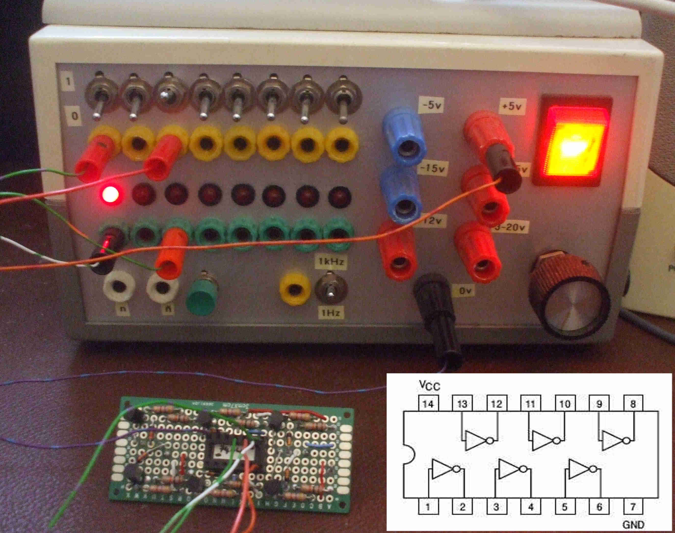
This Minilab has already made an appearance on this website. Here it is being used to power and test my recreation of a 7404 hex inverter.
The Maplin Minilab Kit
Maplin was a British copy of Radio Shack, which also had shops in the UK but under the name Tandy. I lived a bus-ride away from a small Tandy store, a real Aladdin’s cave to the school boy me. Maplin didn’t have many shops at the time but were famous for their big thick catalogues which were sold alongside magazines in larger newsagents.
In this world before the Internet these catalogues were an important reference for hobbyists and their then quarterly “Electronics” magazine showed how all these electronic components could be used to create radios, test gear, etc, etc…
Up to that point I had mainly dabbled with small breadboard circuits but had started to use Vero stripboard so I had some limited experience with soldering. Larger projects however generally required expensive circuit boards or the ability to etch your own, which I didn’t have.
So here it was, a chance to build my own bench PSU and it was designed for Vero stripboard. Maplin provided a kit of parts for £32.50 and a plastic box with an aluminium front and back to house it was (I believe) just under £20. Together equivalent to £120 ($150) in 2020 and a huge investment for me at the time but considering that I left school in 1983 and started college in the same month that the magazine article was published then I no doubt felt I was investing in my education and future.
Courtesy of the World Radio History website a PDF of the original magazine article can be found here on page 16.
I don’t recall having any construction issues but I do remember being nervous about drilling holes to layout the front panel. One miss-measurement or one slipped drill bit and I’d have to live with a wonky front panel because I wouldn’t have bought another.
All went well though and I’ve been proud of this PSU ever since. I owe a huge thank you to the Minilab designer and magazine article author Graham Dixey.
More than just a PSU
To explain the versatility of the Minilab here are its specifications:
A regulated linear power supply providing:
+5V @ 1A
-5V @ 100mA
+12V @ 100mA
+15V @ 50mA
-15V @ 50mA
+3V to +20V @ 450mA (although mine ranges from 2.75V to 23V)
8 x toggle switched TTL outputs
8 x TTL inputs with indicator LEDs
A bounce-free momentary ‘one-shot’ push-button switched pair of complimentary TTL outputs (Q and Q)
A square-wave TTL oscilator switchable to 1Hz or 1kHz
So not the beefiest of PSUs but a useful variety of facilities for experiments that continues to serve me well nearly 40 years later. Even though I now have better PSUs, logic analysers and clock sources the Minilab remains close at hand for quick tests. I should confess though that its longevity has perhaps been helped by one other specification. It sits 11.5cm tall (4.5″) and has a flat top with no air vents – yes, I use it as a base to prop-up my computer monitor! So the Minilab has pride of place in the centre of my desk and I’m still proud to say ‘I made that’.
1993 Improved Version
Roll on 10-years and in June 1993 the Maplin Electronics magazine included an article ‘re-visiting’ the Minilab and improving its design. The new kit (excluding the case) now sold for £49.95
Generally this version reduced component variety and replaced hard to find out-dated components with 90’s alternatives. Component consolidation examples included the use of resistor network arrays, a darlington transistor array and the use of spare NAND gates to form an astable multivibrator to replace the 555 timer of the original for clock signal generation. Further circuit consolidation is achieved with a bespoke printed circuit board replacing the Vero stripboard.
Cosmetic improvements include a front panel adhesive label to identify each socket and a recommendation to use a steel case that included air vents. The voltage regulators are insulated and bolted to this steel case, removing the need for the aluminium heatsink found in my original version.
The de-bounced push button switch has been replaced by a momentary toggle switch to match all the other front panel switches.
The new front panel layout swaps the positions of the clock output and the momentary one-shot output with the switches for each being on the left of their sockets rather than the right. Presumably to aid PCB design and to keep switches away from the PSU voltage output sockets.
Functionally the new unit is almost identical to the original but the +15V output has been sacrificed to provide a new -12V output (+15V is still available via the variable supply). The current available at each voltage level is slightly higher, particularly the variable output that can now deliver up to 1.5A at 24V.
Internally all components tend to have improved specs (e.g. 1% resistors instead of 5%) and all voltage regulators are replaced by newer alternatives, notably the L200 variable regulator is replaced by the LM317T (giving a new voltage range of 1.25V to 24V). So I will assume the later model is more accurate.
The 17V 2A transformer of the original is replaced with a 20V 1A alternative and the single bridge rectifier has been replaced by one for the positive supplies and another for the negative.
With the +-5V regulators now having to dissipate more power if they were connected to the higher incoming voltage they are instead daisy chained from the +-12V regulator outputs. This means the combined 5V and 12V outputs must not exceed 1A.
Possibly the biggest improvement is that the original single 470nF smoothing capacitors on each output (there are none for the variable output) are replaced with 0.1uF and 10uF pairs on every output. This should ensure a much cleaner DC output voltage level, although I have yet to measure just how clean the output voltage of my original version is.
Faults and Improvements
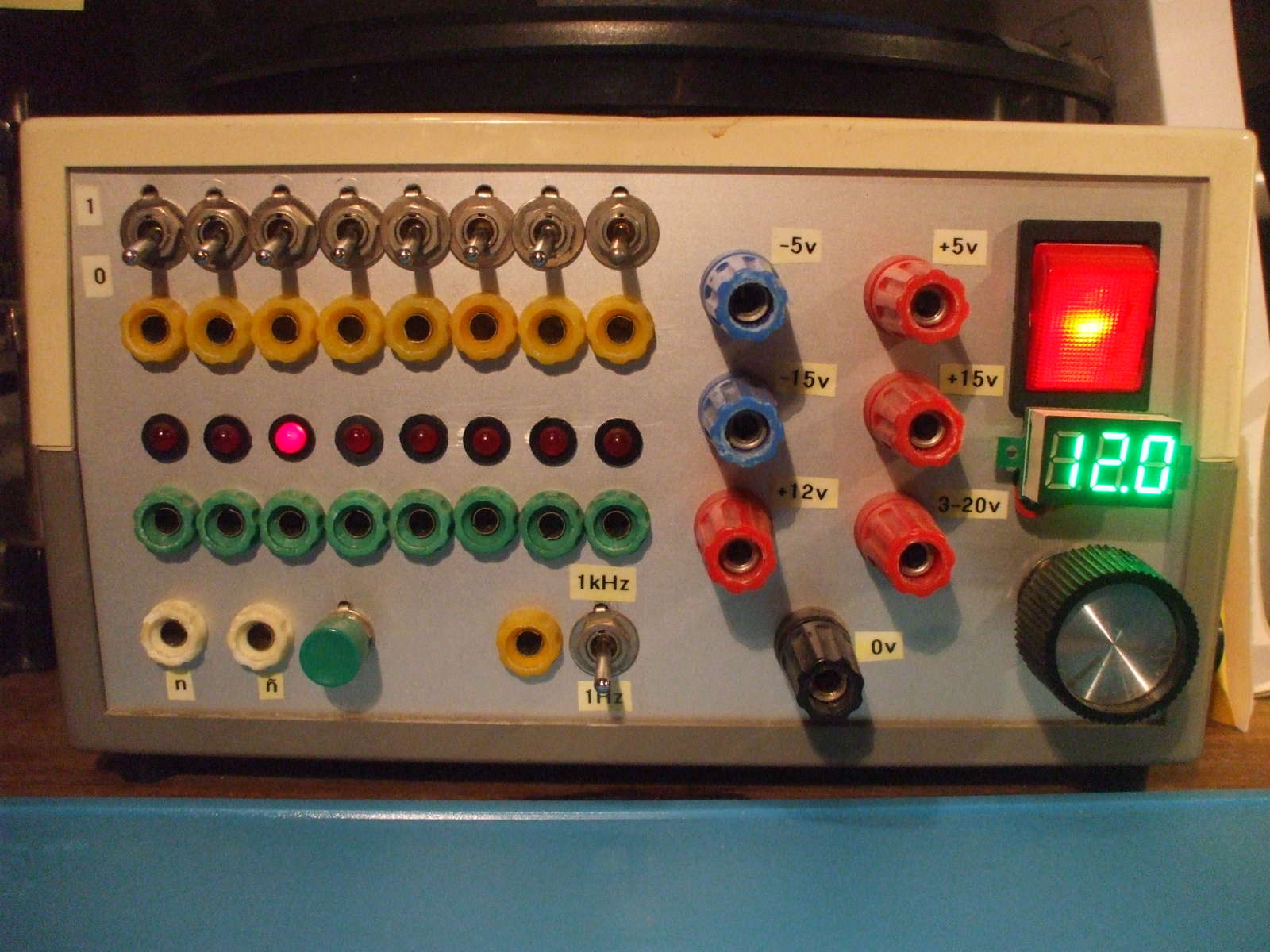
You’ll notice in this photo that sometime since 2015 (when the top photo was taken) I have added a voltmeter to the variable output. This is a cheap module simply stuck to the front panel with velcro. The velcro hides a small hole that allows the 5V, ground and sense wires to pass through the panel and connect to the rear of the relevant sockets (sense to the variable output socket). A simple but useful upgrade. A dual volt/ammeter would be even better but front panel space is tight and I haven’t yet found a suitably sized unit.
You may also notice that my Minilab has developed a fault. One of the logic level indicator LEDs (3rd from left) lights dimly when the Minilab is powered on and nothing is connected (issue-1). This dim light gradually brightens and, as a test, does not go out if that socket is connected to ground?
What you can’t see is that the -5V supply is also faulty, drifting from -8 to -11V or from -6 to -8.5V when under load (issue-2).
My concern about the lack of smoothing capacitors was unfounded though as all voltage levels are appearing clean and with no mains ripple. I’m not sure if they’ll be so stable under a varying load but for my purposes the Minilab has been just fine.
All the other voltage levels are much closer to where they should be and they do not alter when a load is added. +5V measures as 4.9, +-15V as +-14.8, +12V as 12.05. I would prefer the +5V and +-15V to be a smidge closer to their target levels but this isn’t worth tweaking as the Minilab is not intended to be a precision machine. If I should encounter any problems with these voltage levels then I suspect this is due to 4.7k resistor tolerance variations between each output and ground and changing those resistors should get them closer to their intended levels.
There is an issue with the single-shot pulse sockets in the bottom left. Although you’d have to be really pedantic to point out that they’re labelled n and n rather than Q and Q! (my label printer at the time couldn’t do overlines so they’re actually a ‘u’ and an underlined ‘u’ stuck on up-side-down). No, the issue is that they’re wired the wrong way round (or the switch is) and I’ve just got used to that rather than correcting them… The left-hand socket (n) is high with a low pulse and the right-hand n low with a high pulse and really they should be swapped (issue-3).
Having now re-read the original magazine article all these years later I’ve noticed it contains a design option. The variable voltage output is limited to 450mA but by reducing the value of one resistor (R4 to 0.25ohms) on the L200 voltage regulator then that limit could be increased to 2A! That would be useful but it’s also at the limit of the transformer and rectifier so no other outputs should be used at the same time. I think I’ll play it safe and not increase the stress on the old Minilab. If I ever need more current than the Minilab can supply then I know it’s time to use a more beefy PSU.
With a multi-level PSU there is always a danger that different voltage levels can be accidentally shorted (particularly when dealing with positive and negative voltages) and that could then damage their regulators. This hasn’t happened to mine yet (I suspect the -5V issue is caused by something else) so maybe I’m nice and careful or maybe I’m just not adventurous enough? Anyhow, the Minilab lacks any reverse voltage protection so I will try and address that (issue-4).
For completeness and so I have a record of these measures before I start tinkering: The clock outputs both show a 50% duty cycle and range from 0 to 5V in a neat square wave with a rise time of 97nS and a fall time of 17nS. The 1kHz clock is spot on at 1.03kHz and the 1Hz clock measures 0.86Hz, which I can live with as I use it as a slow clock not a precise clock. Although if I did want to make the 1Hz clock more accurate then replacing the supposed 10nF capacitor (C15) with one closer to 10nF or slightly above would do the trick.
The one-shot pulse has a rise of 18nS and a fall of 5.4nS.
Whilst checking all the Minilab characteristics I captured the output voltage levels when the whole unit was powered on/off by its big red power switch. What I found was quite alarming and can be seen in the scope pictures further down this article. Measuring the 5V rail there is a ringing spike of +-12 to 15V at power on and the same at power off. The spikes are very brief and I’ve not knowingly damaged any components with the Minilab but now I know about these spikes I shall be more cautious until they can be resolved (issue-5).
And finally, the mature me should check the electrical safety of the work done by the teenage me (issue-6). Including a check of electrolytic capacitors to make sure they have aged ok.
If I’m going to take the Minilab apart for one of these reasons then I may as well deal with the others to give it a new lease of life.
Repairs and Modifications
Safety always comes first (issue-6) so I’ll start with the last issue by taking the Minilab apart and checking it over. The internal fuse mounted on the right of the Minilab is the correct 1A 250V rating and the plug is wired correctly and has a 3A fuse.

The first thing you’ll notice on the inside is the big mess of wires! As most of these are solid core then it appears quite impenetrable and moving the front panel or circuit board will cause a strain on their soldered connections.
Of more concern though is the curved circuit board which may be stressing some solder joints. It is also bending toward the rear aluminium panel that could have shorted some pins but for a loose clear sheet of plastic between the board and panel, which I shall tape in place.
Attached to the side of the transformer is a sheet of aluminium used as a heatsink for two of the voltage regulators. These regulators do not have any insulated sleeving on their legs. Removing the circuit board could bend these legs into contact with each other or the heatsink so I’ll take the time to reconnect them with some heatshrink protection.
The Minilab’s ground supply is directly connected to mains earth. This is important to check before using a mains earth referenced oscilloscope to test the stability of voltage levels.
Whilst re-soldering fly-leads I’ve also switched the Q and Q cables around (issue-3). They were easier to access than the rear of the push button switch.
I’m still unable to print a Q with my current label printer though so the ‘n’ and ‘n‘ shall remain.
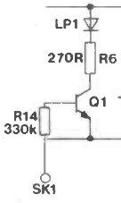
Looking at this extract from the circuit diagram I am expecting a failure of the transistor Q1 is causing the 3rd logic level indicator LED to light (issue-1). A short to ground may also be possible but does not explain the gradual brightening of the LED.
The two resistors measured ok and there were no shorts so I replaced the BC108 transistor with a more modern BC548 equivalent and that 3rd TTL indicator LED now works correctly.
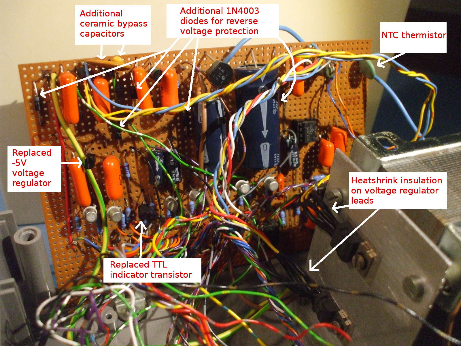
I suspected the -5V supply was drifting down to -11V because the voltage regulator wasn’t grounded but that wasn’t the case (issue-2). So I replaced the 79L05 voltage regulator and I now get a stable -5V supply. I don’t recall what caused this regulator to fail in the first place but one possibility is using multiple voltage levels from the Minilab in a test circuit and accidentally bridging the -5V supply with another. For example the 100mA -5V regulator couldn’t compete with the 1A 5V supply and would suffer reverse voltage.
To prevent a repeat of this I have added protection diodes between each output and ground (issue-4). I used 1N4003 diodes and reversed their polarity so in the -5V example the positive end of the diode was connected to the -5V rail and the negative end to ground. The diode would therefore not short the supply to ground but should a +5V or greater supply be connected then that would be safely diverted to ground rather than to the 79L05 regulator.
There wasn’t space to add these diodes on the rear of the power supply sockets so I found room for each on the circuit board.
Tackling those on/off power spikes proved to be challenging (issue-5). Although I’ve managed some improvement I’m also going to have to admit defeat, for now. I have a lot more to learn about power supply surge protection and hope to re-visit this problem when I do.
These spikes affect all supply voltages but I have focused on measuring results on the 5V supply because that has the potential to damage the TTL components that I have been experimenting with lately. Not wanting to completely re-design the Minilab I limited myself to adjusting existing components or squeezing in more.
Initially I placed a 2A 50ohm NTC thermistor between the transformer output and the bridge rectifier. This ‘negative temperature coefficient’ resistor will reduce its resistance as it heats up. So from a cold start the Minilab will slowly ramp up to full power and therefore eliminate any in-rush current from power-on. This is now noticeable (from a cold start only) as the variable voltage level builds up to its set level in a second or two. But the spike still exists and this thermistor was never going to address the power off spike, no doubt caused by the collapsing magnetic field in the transformer and/or the larger capacitors dumping their charge?
Next I checked all capacitors and tried various additional values between the 5V output and ground. These didn’t have any noticeable effect so I next tried alternative bypass capacitors between the pre voltage regulator supply and ground.
In addition to the 2200uF electrolytic filter capacitor after the bridge rectifier the Minilab uses 220nF bypass capacitors. A bypass capacitor is intended to give any short term voltage spikes a route to ground before they reach the voltage regulators. After several tests I’ve kept the original 220nF polyester capacitor but also added a physically large 10nF ceramic disc capacitor and a physically small 100nF radial ceramic capacitor. Ceramics are supposed to have a quicker response to voltage spikes and a range of bypass capacitor values is intended to filter spikes at various frequency ranges. These do have some effect in reducing the strength and duration of the spikes but from these before and after snapshots you’ll see that the problem still exists.

I’m now losing patience with this problem so will continue to use the Minilab with caution until I can find a suitable solution.
Well I’ve fixed several of the Minilab’s problems and learned a lot more about it than I did in 1983. This photo shows the mess of my teenage creation with some of my recent modifications labelled.
I’ve decided to categorise the Minilab as Silicon Heaven despite building it myself. Hundreds of Minilabs must have been created but I wonder how many are still operational?
This was a popular kit but is now rarely mentioned. Nowadays it’s fairly easy to turn a PC power supply into a bench PSU but the IBM PC was still new and expensive when the Minilab was published and it took many more years before they became available for recycling. For many of us, building the Minilab was essential and affordable.
Sadly Maplin, like Tandy, evolved into being just another generic retailer and forgot their hobbyist roots. Both went bust but their names continue to trade as online stores.
Categorised as: Electronic Stuff | Silicon Heaven
Comments are disabled on this post