Logic buffers —
With computer programming I’m drawn toward low level languages. Somehow hoping to understand what all the 1’s and 0’s are doing to truly feel in control of the computer.
An understanding of those basic building blocks is really important even though using them in most projects would be too time consuming and error prone.
With electronics I find myself in a similar position. Using microcontrollers and other integrated circuits (ICs) but still keen to understand what those 1’s and 0’s (or +5v and 0 volts) are really doing.
So I thought I’d have a dabble with some simple logic circuits, the basic building blocks of digital electronics.
As usual I should point out that I am no expert and what follows are just notes of my tinkering. Written in the vain hope that some of it may actually stick in my brain. Or if it doesn’t then at least I’ll have something to refer back to.
If any of this piques your interest in electronics then great but please please get a book and learn from the experts.
Let’s Hit The Buffers:
In logic terms I thought these may be a nice and simple example to start with. Or at least I assumed the electronics would be simple, explaining a buffer may take a bit more effort.
Firstly ‘buffer’ is a common term in programming and electronics and can be used to mean different things. What I shall try to explain here is the simple digital logic buffer not the sort that holds input or output until your circuit or program is ready to deal with it.
ICs come with buffered or unbuffered inputs but what does that mean? Well, here goes…
Unbuffered input means the incoming signal is fed straight into the IC’s internal circuits. Not a problem if you trust the source of the signal but what if it’s too weak to drive the IC or too strong and therefore potentially damaging to the IC.
Buffered input tries to mitigate these risks by offering some protection (within reason) and by reinvigorating the signal to a level that the IC will be happy with.
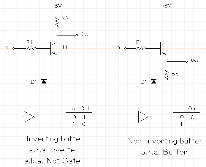
Non-Inverting Buffers:
A non-inverting buffer does nothing, in logic terms. The output logic level will be the same as the input logic level but remember the protection and re-invigoration of the input signal. So a non-inverting buffer does do something.
Also the way the buffer slows a signal can be used to good effect by helping to keep multiple digital signals that may run through different logic circuits, and therefore slowed at different rates, in sync.
Inverting Buffers:
An ‘Inverter’ circuit is almost identical to a non-inverting buffer but the output is the opposite logic level to the input. In logic terms an inverter is a ‘not gate’. When the input is on the output is not on, when the input is off the output is not off.
In fact two inverting buffers in series, with the output from one being used as the input for the next, is another way of creating a non-inverting buffer.
Example Circuits:
Here are some example circuits for the non-inverting and inverting buffer along with their respective logic symbols and a table to show what output each circuit would produce for each input signal.
Having struggled to produce neat circuit diagrams in the usually wonderful Fritzing I eventually resorted to, and was impressed by, XCircuit to produce these.
To make and test these circuits on a breadboard I used whatever components I had to hand:
T1 – I had a bag of BC546 transistors, designed for amplification but ok for manual on/off switching and also at my modest test frequency of 1kHz. It’s T1 that does the magic in this circuit. When sufficient voltage (see Logic Levels below) is applied through the ‘in’ signal to the base of the transistor it ‘switches’ on and allows current to flow from the +5v supply to ground (ok, I know current actually flows in the opposite direction but let’s not confuse matters when the circuit symbols suggest otherwise).
For the inverting circuit this redirects the voltage away from the output (so output is off when the input is on and vice versa). For the non-inverting, voltage is only applied to the output when T1 is on and so output is also off when T1 is off.
R1 and D1 – are my limited attempts at circuit protection. For R1 I used 10KΩ. R1’s job is to limit the current flowing into the base of T1 to protect it from burning-out. For D1 I used a small signal diode, probably a 1N4148. D1’s job being to protect T1 from any negative voltage levels on the incoming signal by routing them to ground.
That leaves R2 – R2 provides some protection to the current flowing through T1 when it is switched on but it also plays a part in shaping the output signal. I used an oscilloscope to observe the shape of the output signal for different values of R2 when applying a 1kHz square-wave signal to the input. I settled on a value of 4.7kΩ to produce a neat square output. Higher values produced a slower reaction to the switching on/off of T1 which resulted in distortions to the square shape of the signal (rise and fall were not vertical). Lower values were ok for signal shape but I assumed they would be letting too much current flow.
I would assume that the optimal value for R2 would depend on signal frequency and the logic voltage level.
Logic Levels:
Testing the voltage of the output signal I would understand if you thought something was wrong. It being 0v for a logic low (i.e. a ‘0’) and around 4.3v for a logic high (a ‘1’). But shouldn’t the high be 5v?
Well no, not for these circuits anyhow because some of the voltage will be dropped by T1. However, 4.3v is ample for driving other circuits operating at +5v logic. For 5v logic anything over 2v is considered high and anything below 0.8v a low. Anything in between 0.8v to 2v is unreliable and could trigger either level, so best avoided.
By testing the input voltage required to switch on T1 I found this was as low as 0.8v. Now that may be considered too low for reliable operation but I’m happy that will be fine for my simple test circuit. Especially as it would be sensitive enough for use with Raspberry Pi 3.3v logic level input whilst still providing a suitable 5v logic output (which must not be fed back to the Pi! but is fine for an Arduino).
Now if I’d wanted to adjust sensitivity to the incoming logic level I could add another resistor (R3) between the base of T1 and ground (parallel with D1). R1 and R3 then act as a voltage divider. The larger R3 is in proportion to R1 then the more sensitive the circuit is (i.e. the lower the voltage required to switch T1 on). If R3 is the same as R1 then the incoming voltage to T1 is halved, meaning an incoming voltage of around 2v is required to switch T1 (close to the expected 5v TTL level).
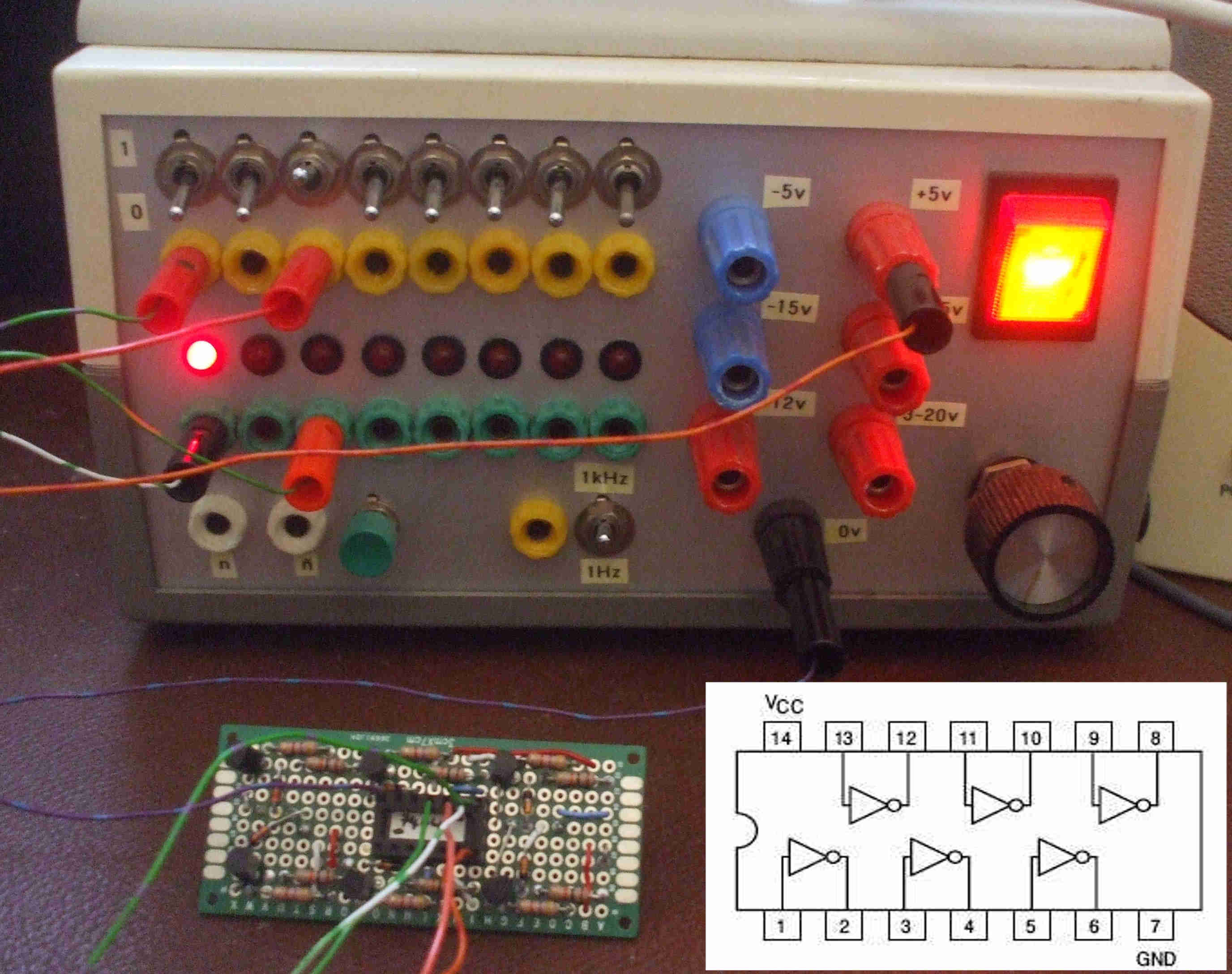
Making A Hex Inverter:
Breadboard circuits come and go and are soon forgotten. I wanted to make something permanent but a single buffer circuit would be a waste of a small circuit board. So I decided to make an RTL (resistor transistor logic) equivalent of a very common TTL (transistor transistor logic) IC, the 7404 hex inverter. It’s called ‘hex’ because this particular IC contains six inverting buffers in a 14 pin chip (two pins per buffer for input and output, one for the 5v supply and one for ground).
By ‘equivalent’ I mean mimicking the pin-out and basic function of the 7404. I couldn’t hope to match the characteristics or performance of the actual chip nor copy its internal circuitry which contains some 30 transistors, 36 resistors and 12 diodes. My version would contain just 6 transistors, 12 resistors and 6 diodes, being simply six copies of the previous inverter circuit.
I had some 10×24 hole double-sided perfboard (I’ve used stripboard before but not perfboard) and initially thought of placing single sockets at equal spacing around the edge to copy the 7404 pinout. But those sockets wouldn’t have been very stable so I thought I’d group them together in the middle of the board. I then realised that the neatest and most stable solution that best mimicked the IC would be to use a 14-pin IC socket.
I struggled to use Fritzing (again) to display my design because my small board layout is rather congested and Fritzing only offered a single-sided perfboard option. So here is a photo of my completed board which should change to a hand-drawn circuit diagram if you hover your mouse cursor over the image. It may take a couple of seconds for the new image to load for the first time but once cached you can then quickly switch between the photo and circuit diagram by moving the mouse cursor on/off the image.
On the diagram you will hopefully spot the six copies of my earlier inverting buffer circuit

Now remember this is my first time with perfboard! I was definitely getting neater as I progressed but decided against creating a second board just for vanity reasons. This works ok (well it didn’t at first, hence the diagonal diode on the right-hand side because the original was faulty) but it’s good enough for the simple logic examples I may use it for.
To be honest I’ll most likely use an actual 7404 but at least I can now appreciate what’s happening inside the chip!
And here is the actual 7404 pinout along with my version which is connected up to a homemade logic tester. Note for the two connected switches and their corresponding LEDs that an LED is on when the switch is off and off when the switch is on. i.e. their signal has been inverted.
Well digital electronics doesn’t get much simpler than the logic of buffers although, as suspected, explaining the electronics is more difficult.
Testing these simple circuits on a breadboard and trying different component values before finally soldering the hex buffer circuit board has certainly etched what I’ve learned onto my brain. I now feel like having a go at making some other types of logic gate.
Categorised as: Electronic Stuff
Comments are disabled on this post