8-Bit CPU – MMU —
A Memory Management Unit for my 8-bit “Hol-1” CPU
Why an MMU?
An MMU controls a computer’s memory. On a larger more complex CPU this would involve ‘virtual memory’, security and the fine-tuning of memory organisation. A clever part of CPU architecture that helps even inefficient software to perform reasonably well.
With only 64-bytes of memory in the Hol-1 RAM this MMU is not going to be complex or clever.
An MMU would normally initiate memory I/O and provide a flag to the CPU when it was complete. This is because the I/O could take an indeterminate amount of time and cannot be assumed to complete within a set number of clock cycles.
The slowness of Hol-1 and the relatively speedy 74LS189’s used on the RAM board however mean that I am expecting memory I/O to complete within a single clock cycle. So such a flag will not be needed. If I later have timing problems then I’ll have to insert some pauses into programs to allow memory commands to safely complete but I doubt that will be necessary.
My RAM board can receive memory input and output commands but it requires two simultaneous data streams to perform them. One to identify the memory address and another to convey the data to be stored or recovered from that address in memory. But as there is only a single Data Bus on Hol-1 the CPU can only transfer one data stream at a time and not the two that the RAM requires.
This problem is resolved by the MMU but to do so it will require all memory commands to be in two stages (i.e. 2 clock cycles). The first to convey the memory address across the Data Bus to the MMU for storage and the second stage to convey the memory data across the Data Bus. The MMU can then present the RAM with both address and data streams at the same time.
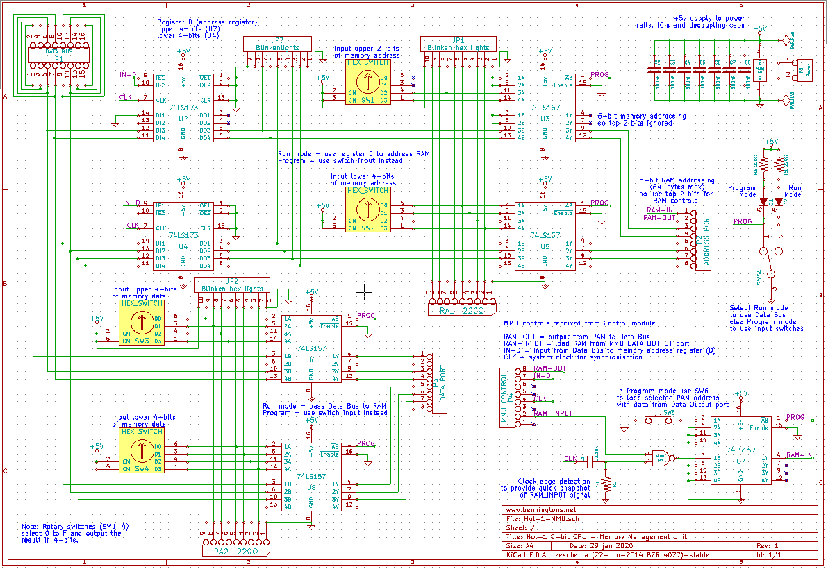
So the MMU needs to store the requested memory address and it does this in the Address Register. As Hol-1 already has A, B and C registers I will refer to the Address Register as register D. This will make the future mnemonics of a Hol-1 assembly language less confusing.
Is the Hol-1 MMU just an Address Register? Well you’ll see from the Hol-1 Register board that the 8 x 12cm circuit boards used to build this CPU can hold 3 registers. So an MMU that just holds an Address Register would be rather empty.
To utilise the remaining space a ‘programming’ interface has been included on the MMU board.
With address and data paths to RAM going via the MMU there is an opportunity to interrupt normal operation and to allow the Hol-1 user to change the contents of any memory location. This could be used to input data into a program or to update sequential memory locations to input a program into Hol-1 RAM.
[Although at this stage I’m expecting Hol-1 to execute programs read from an EPROM, it could also be feasible to read instructions from RAM.]
Basic Design:
The MMU requires a connection to the 8-bit Data Bus, two ports for conveying address and data simultaneously to the RAM board and a port through which it can receive signals from a control board.
Just four control signals are needed:
IN-D: An instruction to store the contents of the Data Bus into register D (Address Register).
RAM-INPUT: An instruction passed onto the RAM board to store the contents of the data port into the memory address indicated by the contents of the address port. A NAND gate is used to convert this logic high signal into the brief logic low pulse required by the 74LS189’s on the RAM board.
RAM-OUT: Also passed to the RAM board to instruct it to output the contents of the memory address indicated by the address port to the Data-Bus.
CLK: And the Hol-1 clock signal to synchronise the above actions.
Because Hol-1 only has a 64-byte RAM, only 6-bits are needed to address all memory locations. Therefore, as I’ve standardised on using 8-bit inter-board links, I’ve used the remaining 2-bits on the 8-bit address port to pass the RAM-INPUT and RAM-OUT commands onto the RAM board.
The Address Register (register D) will be a repeat of the design for registers A to C but unlike those initial registers, D will not be able to output to the Data Bus. The Address Register will instead provide a permanent output via the address port to the RAM board. This means the blinkenlights display on the RAM board will always display the contents of the memory address identified in the Address Register. I’ll also add a blinkenlights display to the MMU to show the value held in the Address Register. You can never have too many blinkenlights.
This leaves the ‘user interface’ aspect of the MMU to be defined.
RUN/PROG mode: A toggle switch to change between normal (run) mode and programming mode. This switch will cause four 74LS157’s to swap user selected inputs for the usual Address Register and Data Bus outputs to the RAM board. It will also disable the RAM-INPUT signal to allow the user to select when to write to memory.
Binary input: User selected input for the 6-bit address and 8-bit data to store in RAM.
LOAD button: A momentary switch to signal that the user selected binary input is to be stored in RAM.
Construction:
I intended to use traditional rocker or slide style DIP switches for the binary input of address and data but found them too fiddly to use when prototyping the MMU on a breadboard. They’re okay for occasional input but you wouldn’t want to frequently use them. So I considered using a hex keyboard or a panel of larger toggle switches instead but wanted to keep Hol-1 on 8 x 12cm circuit boards.
Eventually I discovered rotary DIP switches and a hex version made by APEM (the PT65 series). Not cheap (by my standards) but an easy to use finger & thumb rotary switch with a 0 to F selection that would output the corresponding binary value. e.g. select 9 and the output will be 1001, A=1010, B=1011, etc…
The high or ‘1’ values are selected by the rotary switches and 220R resistor arrays are used to pull-down the unselected values to low or ‘0’.
A pair of these rotary switches will be used to set the data value to input to RAM and another pair will set the address value. The top two bits of the address value will be ignored as only 6-bits are needed to identify each of the 64 memory addresses.
Although the 0 to F value on each rotary switch shows the value selected a couple of blinkenlight LED arrays have been added to display these values in binary form. All Hol-1 boards have used these displays by providing a line of 8 data pins alongside a ground pin for the blinkenlight module to plug into.
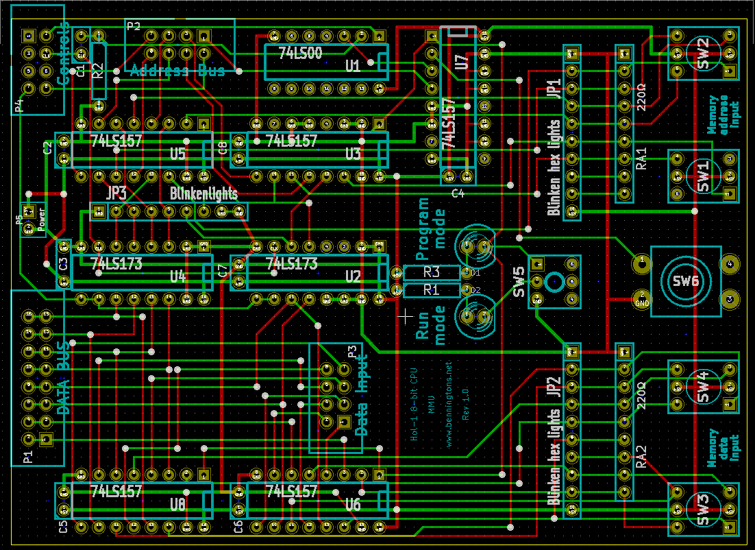
Usually I try and keep IDE sockets around the edge of a board to prevent ribbon cables trailing over and obscuring the PCB. Sadly on this MMU I’ve ended up placing an 8-pin Data Input socket in the lower centre of the board. I hope I won’t later regret this but space is limited and I didn’t want any cables getting in the way of the rotary switches and programming buttons.
To switch from RUN to PROG mode I’ve used a latching push button (SW5) alongside a green (RUN) LED and an orange (PROG) LED to show which is currently selected.
The LOAD button (SW6) has been placed on the edge of the board between the two sets of rotary switches. I’ve thought about the ergonomics of using these buttons and believe this is the best I can do in the space available.
Parts List:

80x120mm 	double-sided prototype PCB (a.k.a. perfboard)
R1, 3		220R
R2			1KR
RA1,2		220R single-in-line (SIL) resistor arrays
C1			Ceramic Capacitor 10nF
C2-8		Ceramic Capacitor 100nF
D1			Orange LED
D2			Green LED
IC1			74LS00 quad 2-input NAND gates
IC2,4		74LS173 4-bit flip-flop, tristate with asynchronous clear
IC3, 5-8	74LS157 quad 2-line to 1-line data selector, non-inverting
SW1-4		rotary hex switches (APEM PT65 series)
SW5			latching push button switch
SW6			momentary push button switch
8 x			14 and 16-pin IC sockets for the above ICs
1 x			JST PH 2-pin male connector (for power supply)
3 x			8-pin (2 rows of 4) male IDC box headers (for control, data and address ports)
1 x			16-pin (2 rows of 8) male IDC box header (for Data Bus connection)
2x10 and 1x9 rows of male header pins (for blinkenlight plugin modules)
and various 26 to 30AWG wires.
For an indication of the cost, the total for all the above parts was about £15 ($19 USD) making this the most expensive Hol-1 board so far. Although £11 was for the rotary hex switches which could be replaced by dip switches for less than £1.
Testing:
It’s been a few months since I’ve had time to work on Hol-1 so I started by re-testing all the boards constructed so far. I did this by first noting what value to expect on every pin of every IC on every board and then using a logic probe to confirm if all was as expected.
I did find some intermittent errors and finally tracked these to some poorly crimped JST sockets that I’m using for power distribution. I’ve concluded that buying pre-crimped wires of any kind is a false economy. Even if they initially test okay there’s a possibility that they later fail when wires get moved about. I shall start crimping my own and mistrusting all others.
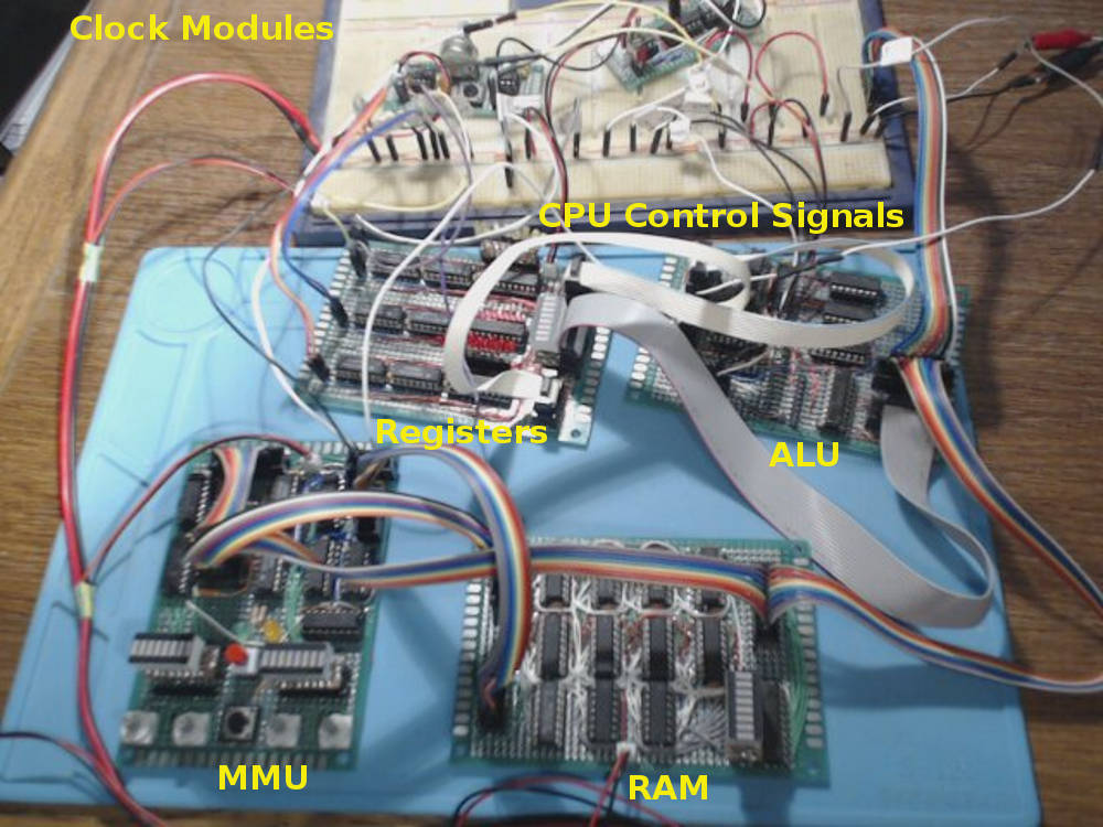
To soak test all boards I set the MMU to RUN mode (green LED) and enabled the following commands:, INC, ADD, SUM-OUT, A-IN (to get the A register counting up in steps of 1), D-IN, RAM-IN (to save 1 in memory address 1, 2 in 2, etc…). Later I disabled RAM-IN (to continue displaying the contents of each memory location, which would continue to be 1 in 1, 2 in 2, etc…).
This could be left indefinitely and worked well.
As stated previously in my Hol-1 RAM blog the RAM chips feel slightly warm but this appears to be normal.
To test the user input capability of the MMU I first pressed the latching switch (SW5) to set it to PROG Mode (orange LED). I could then dial numbers on the rotary switches (SW1-4) and press the LOAD button (SW6) to store the selected data value into the selected memory address.
Rotating back the address rotary switches to previous values showed that previously stored values were still held in memory (displayed on the RAM board’s blinkenlight array).
I don’t want to give the impression it worked first time though. Some minor soldering corrections were needed and R3 was a late addition to get program mode working properly but now the MMU appears to be working okay.
When I completed the RAM board, total Hol-1 power consumption was 730mA. Now it is 1.3A or 1.15A without any blinkenlights. As all appears to be working then I shall live with that but I suspect that sooner or later I will have to improve this.
Improvements?
I hope that any future CPUs I make will include some form of external keyboard or at least a control panel for a user interface. But given the limitations of Hol-1 this MMU appears to be the best I could have hoped for.
The potential to provide a D-OUT command to place the contents of the Address Register onto the Data Bus could be useful but a new ALU with flexible inputs from any register would probably be a better choice.
Expansion to full 8-bit addressing (256 bytes) by using four RAM boards and the top two bits of memory to select one of them from the MMU would be possible but probably not in the space available.
An improvement that I would like to implement is to swap the binary blinkenlight display of values from the rotary switches into hexadecimal displays. I’ve added a 5v pin to the line of data and ground pins for these plugins to help support this and reserved some board space around them for a larger display. I plan to use a plugin with a binary to hex decoder and some 7-segment LED displays. More on that to follow in a future post.
Categorised as: Homebrew 8-Bit CPU
Comments are disabled on this post