8-Bit CPU – RAM —
Adding a RAM board to my 8-bit “Hol-1” CPU.
What is RAM?:
Continuing the build of a simple CPU from TTL chips the next step is the random access memory (RAM). It’s not ‘random’ because it’s haphazard but because you can read/write to any section of memory directly using its address. Historically memory devices had to be accessed sequentially from beginning to end until you reached the address you needed. Sequential access memory still has its uses today but it’s too time consuming for a CPU that needs to frequently access individual bytes of data in any order required by a program.
RAM is somewhere to store a program and data. We also have the A, B and C registers to hold data and they can process it through the arithmatic & logic unit (ALU) but they only hold 3 bytes. RAM can be used to store far more but the downside is that it takes time to move data between the registers and RAM. Another overhead is the need to provide an address to identify which byte of memory you wish to access.
The Basic Design:
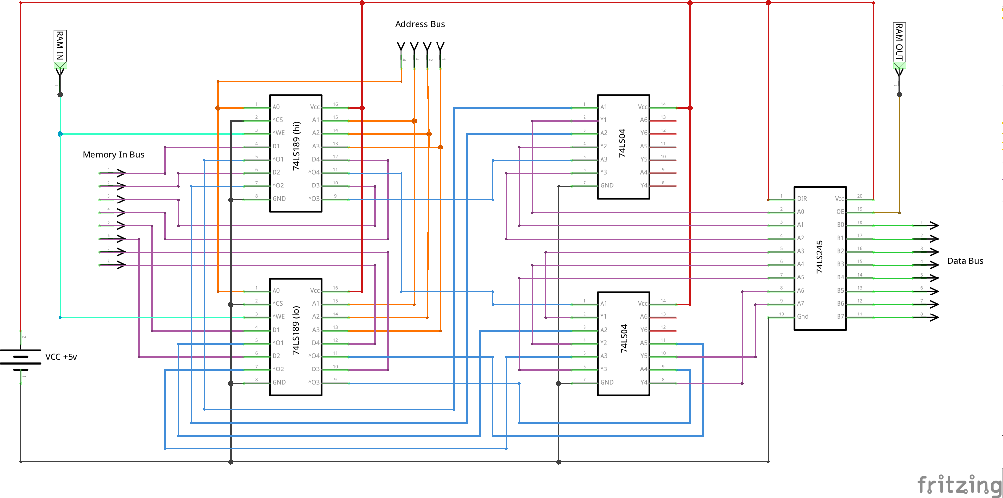
The 74LS189 provides 16 addressable slots of 4 bits each. So using two of these chips in tandem provides 16 addressable bytes of 8 bits each.
A 4-bit address signal is needed to address each byte. That’s 0000, 0001, 0010, …, 1111 in binary or 0 to 15 in decimal. Feeding that address to both chips simultaneously ensures the two halves of each byte are written or read in the same corresponding address on each chip.
A downside of the 74LS189 is that the output is the inverse of the byte stored (actually it’s the inverse of the byte written to memory that is stored). So you could write 11001010 to these chips but 00110101 would be read back. I presume that may be useful in some circuits but to correct this a couple of hex inverters (74LS04’s) are used. The 74LS04 has 6 (hex) inverter gates per chip to switch 1’s back to 0’s and vice versa. That’s 12 inverters available so 4 will not be needed.
A tri-state buffer (74LS245) is used to control whether the RAM output is fed to the Data Bus or not. As used in the previous Register and ALU boards these ‘tri-state’ buffers can read or write to a bus. That’s two states and their third state is that they can disconnect from the bus and so not interfere with signals if other chips use it.
However the Data Bus is not used for bi-directional I/O to this RAM board, it is only used for RAM output. An 8-bit Memory-In Bus is used for data input to enable direct programming of memory from a separate board (which I’ll do next and probably amalgamate with the Address register). So the 74LS245 is set to output only (direction pin 1 always held high) and that is triggered whenever pin 19 is low.
This basic design eventually worked on my breadboard but the usual mess of wires meant the circuit was not easy to follow and each time a wire was knocked the circuit would misbehave. I wanted to solder a permanent circuit but first I needed to address the issue of memory size. This may be a simple TTL CPU but 16 bytes for both program and data was not going to be enough.
Schematic:
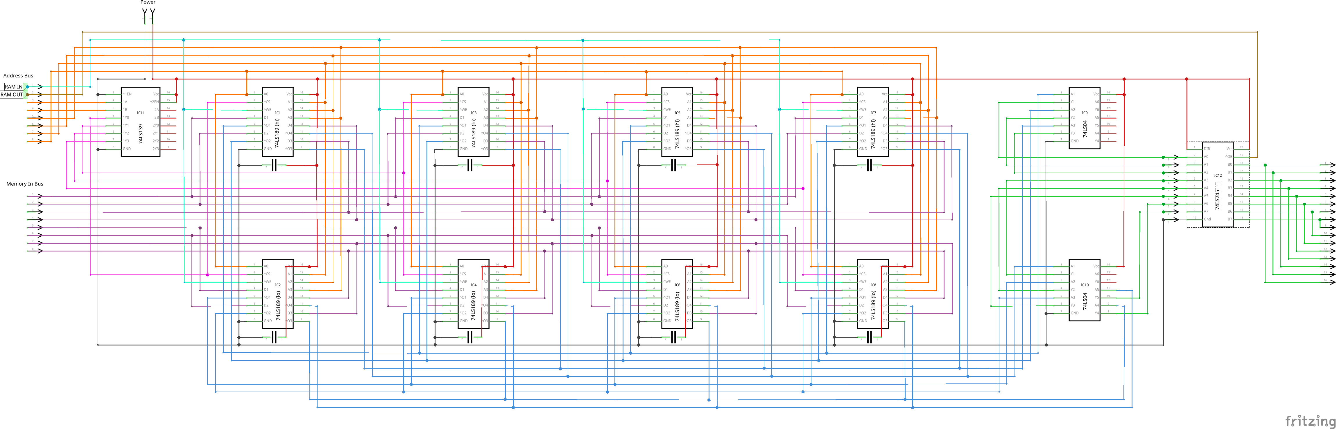
Because 16 bytes of memory isn’t very useful I expanded the initial design to 64 bytes by adding 6 more 74LS189’s. So that’s 4 pairs of 74LS189’s with 16 bytes in each pair = 64 bytes of memory in total, far more useful than just 16.
To address this extra memory I’ve expanded the Address Bus from 4 to 6 bits. The top 2 bits of this Address Bus can then be used to select one of the 4 memory pairs as 2 bits can hold 00, 01, 10 or 11 – that’s 4 values or 1 to address each pair of memory chips.
To decode the top 2 bits of the Address Bus and determine which of the 4 pairs of memory to use I’ve added a 74LS139 (2 to 4 line decoder). This takes the two additional address bits as input and provides an output of 1110, 1101, 1011 or 0111 – which is used as a signal to turn on one of the memory banks whilst turning off the other three. i.e. each bit of this output signal is fed to the chip select (pin 2) of a corresponding pair of 74LS189’s. Turning one bank on (because chip select is active low) whilst turning the others off.
The bottom 4-bits of the Address Bus still goes to the address input pins of the 74LS189 (all eight of them) but the top 2-bits of the Address Bus (via the 74LS139) selects which pair is enabled to receive or output data.
I should note here that I was tempted to use alternative memory chips to provide a RAM of larger capacity. This would have been easier and could have been achieved with a single memory chip but it would have been anachronistic to the rest of my simple TTL CPU design. i.e. If the rest of the CPU uses chips that were prevalant in the late 1970’s then so should the memory.
Back in those days it was easy to spot the memory board of a computer because it was heavily populated with the same model chips (I’m thinking PDP-11). So I wanted this RAM board to look similar, although on a much smaller scale.
As with previous boards I’m getting nervous about power supply affecting logic performance. i.e. slow rise times from 0 to 5v causing a curved rising edge to what should be square wave signals. At best this would reduce the maximum clock speed of the CPU and at worst it would affect accuracy because signals spend too long in the grey area between logic high and logic low, meaning they could be interpreted as either.
To address this I’ve added 100nF capacitors below and across the power supply rails of each memory chip in the schematic. These should assist the chip by providing a local current source for short bursts should the power supply be slow to respond. Whether 100nF is enough and whether a larger electrolytic capacitor per board is required will be determined through testing. Capicitor upgrades or additions should be easy to accommodate on the final circuit board.
I’ve only provided one set of 9 header pins for a blinkenlights module on the RAM board. This is placed prior to the 74LS245 buffer so that the contents of the memory address fed to the Address Bus can be displayed even if we don’t wish to output that to the Data Bus.
With the Programming Board displaying the state of Memory-In Bus and Address Bus there was no need for more blinkenlights on the RAM board.
Finally for the schematic I don’t need to explain the purpose of the two control signals for this RAM circuit, RAM-in and RAM-out. Each will trigger an action when they drop to logic low (0v).
Having just two control signals and a 6 bit Address Bus means they can neatly share an 8-way ribbon cable which I’ve been using as a standard for single board to board connections (apart from the Register board which is now annoying me, I may have to do a mod on that…). For bus connections to multiple boards I’m using 16-way cable to allow for an easy implementation of a 8-bit bus hub (currently on the ALU board).
Construction:
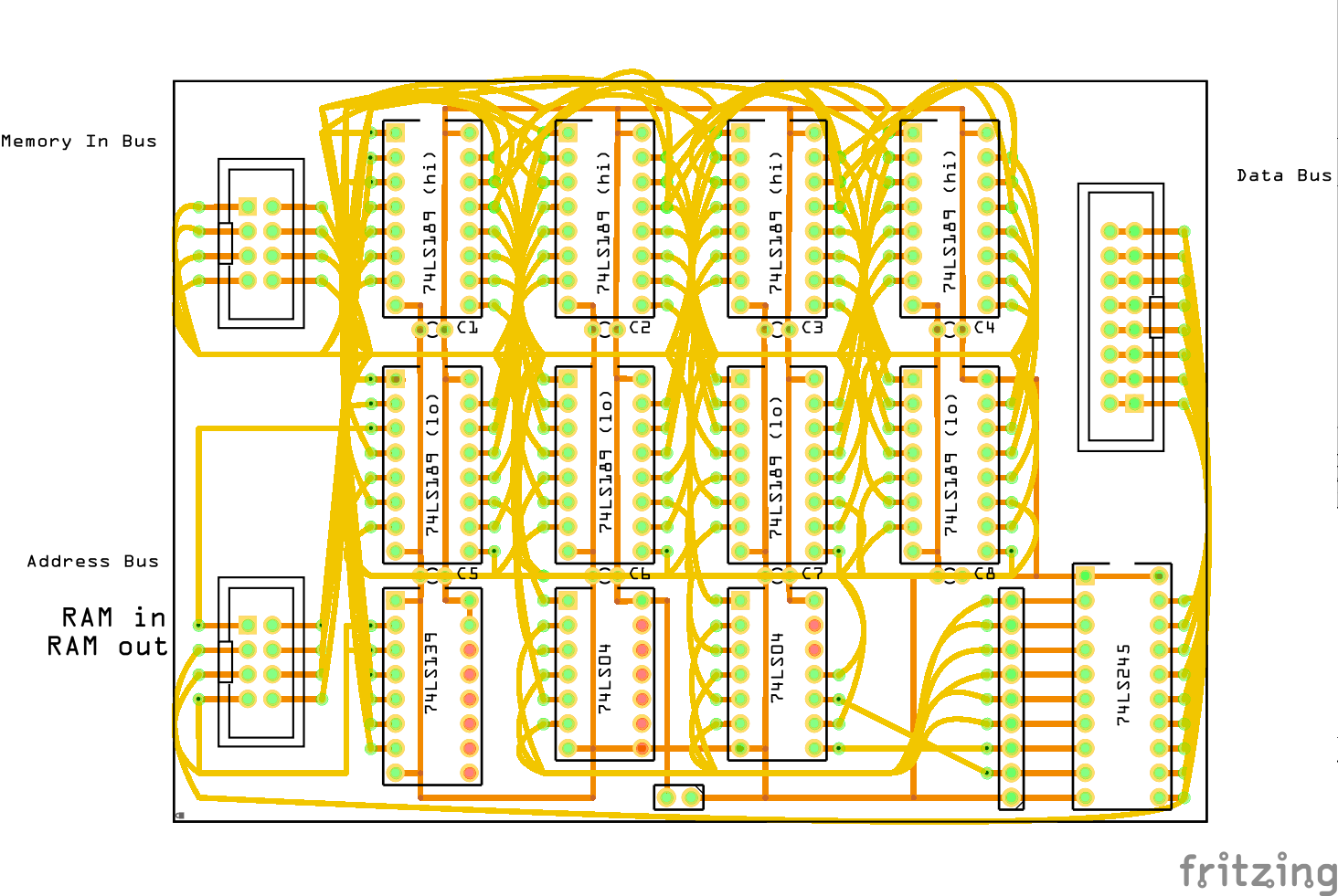
This circuit board layout shows the component positioning although their congestion means the connecting wires cannot be followed (see schematic above instead). I will also look at publishing all Fritzing files onto GitHub.
The circuit is laid out on the same 8cm x 12cm double-sided perfboard that I’ve used for the previous CPU boards. It’s congested and because of that I had to sacrifice capacitors C5 to C7 when building the board. It was my folly to try and keep a neat layout with all chips in the same orientation. If I had placed the inverters at right angles to the memory chips and moved the 2 to 4 line decoder to between the two input buses then they could have stayed. If I experience power issues affecting the sharpness of the logic signals then I shall mod the board to squeeze in some additional capacitors.
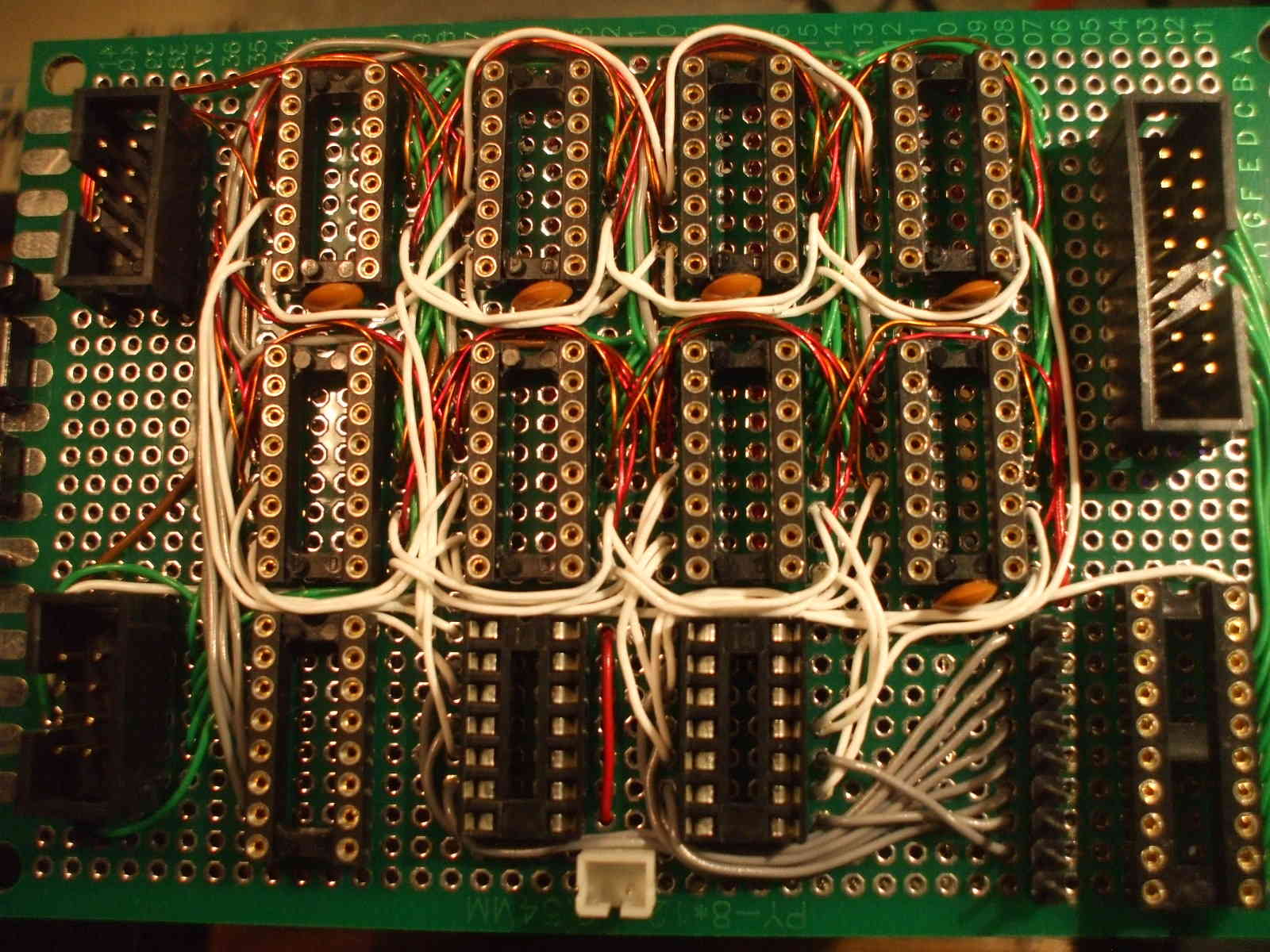
As with previous boards I have continued to use enameled copper wire salvaged from an old transformer for the on board data in lines. I believe that to be 28AWG and the coloured wires used for other lines range from 26 to 30AWG. The latter in cases where the congested design required more than one wire to pass through the same 1mm perfboard holes.
Parts List:

80x120mm double-sided prototype PCB (a.k.a. perfboard)
C1-8	Ceramic Capacitor 100nF
IC1-8	74LS189 64-bit RAM (16x4), inverting outputs
IC9-10	74LS04 hex inverter
IC11	74LS139 dual 2 to 4-line decoder, inverting outputs (only 1 of the 2 decoders are used)
IC12	74LS245 8-bit bus transceiver, non-inverting, tristate (i.e. on, off and disconnected)
12 x	14, 16 and 20-pin IC sockets for the above ICs
1 x		JST PH 2-pin male connector (for power supply)
2 x		8-pin (2 rows of 4) male IDC box headers (for ribbon cable direct link connections)
1 x		16-pin (2 rows of 8) male IDC box header (for ribbon cable bus connections)
1 x		row of 9 male header pins (for a blinkenlights module on the RAM output)
and various 26 to 30AWG wires.
For an indication of the cost, the total for all the above parts was less than £6 ($8 USD).
Testing:
As I hadn’t breadboarded the full 64 byte circuit, only the basic 16 byte portion, I was concerned about committing so much time to create the board. But in theory it should work and in practice it did, eventually…
The design and construction of the RAM board itself turned out to be OK. The problem was that previous boards (Registers, ALU and Clock) were misbehaving? They passed their tests in isolation but when all were connected their behaviour was unreliable?
This indicated a power supply issue from their collective drain. Till now I’d been using an old 5v mobile phone charger rated at 550mA and the growing CPU must now be drawing more current.
I switched to using a homemade bench PSU that provided 5v rated at 1A and the partial CPU performed ok. But when left on a soak test it started to become erratic after a minute or so.
Switching to a 2.1A PSU I measured the average current drawn as 730mA so my bench PSU should have been ok (it’s either below spec or the supply leads were too long).
When under a soak test I’ve noticed the memory chips feel warm and all the other boards remain cool to touch. This isn’t a concern yet and perhaps the norm for a CPU of this generation. Despite the 74LS range standing for Low power Schottky they draw a current of 1,000+ times more than a modern logic chip.
To test the RAM board I’ve needed to use all the boards I’ve created so far (Clock, Registers and ALU) plus a breadboarded version of my next HOL-1 board. That being a combination of the address register and Programming board (I’ll add a link here when that has been completed as a circuit board.
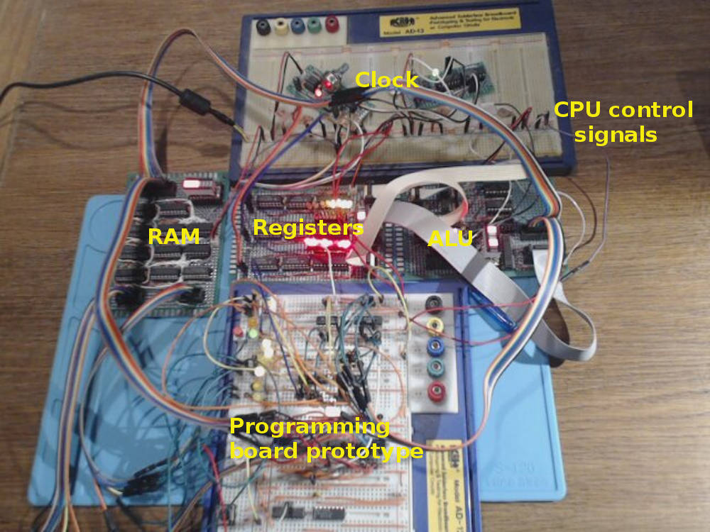
The Programming board enables me to set values on the Address and Memory-In Buses using some DIP switches. I can also bypass those switches and use the Data Bus instead.
So initial testing comprised of selecting individual memory addresses across the available 64 byte range. Inputing data into each of those addresses by setting RAM-In low and then returning to each address and checking the same value can be output to the Data Bus by setting RAM-Out low.
This worked ok (after resolving the power supply issues) but was tedious to operate with the small DIP switches. I shall have to look for an alternative programming interface when making that next board.
To speed up the testing of all memory addresses and to provide a soak test I first set the ALU to increment the A register and the A register to read in the result. i.e. I created a loop where the A register would count from 00000000 to 11111111 and then continue to repeat that.
With that counter running I then set the Address Bus to the Data Bus and the Memory-In Bus also to the Data Bus. With Ram-In set low the value in each memory address was therefore set to the number of that address. (Well actually with the Address Bus only being 6 bits the value stored could have been higher i.e. address 110011 could be holding 00110011, 01110011, 10110011 or 11110011)
Once all 64 bytes of RAM were loaded I set the RAM-In high and kept RAM-Out high. I could then leave the partial CPU to soak test with the ALU incrementing Register A and that value on the Data Bus would cause the RAM board to display the contents of that memory address on the Ram board’s blinkenlights. Note that this enables us to peek at each memory address but we’re not outputting the contents onto the Data Bus (RAM-Out is high) as that would interfere with the counter process between Register A and the ALU.
With the RAM board finally completed my next challenge for this “HOL-1” 8-bit CPU is the Programming Board. As that has largely been completed on breadboard to enable the RAM board to be tested then hopefully that won’t take too long.
Categorised as: Homebrew 8-Bit CPU
Comments are disabled on this post