8-Bit CPU – Registers —
Building CPU registers with TTL logic and some blinkenlights.
Recap:
Previously I posted about my quest to build a computer’s central processing unit (CPU) from transistor transistor logic chips (TTL). This initial venture into CPU design being very much guided by Ben Eater’s video tutorials for a computer built on breadboards. Please refer to Ben’s videos for a thorough explanation of how a computer works. I shall instead focus on my design modifications and a more permanent project build using circuit boards.
Having completed modules to generate and control a suitable clock signal my next step is the registers. These hold data within the CPU for processing purposes, being faster to use than data held in memory these registers will also be directly referred to by commands in the instruction set.
On a Breadboard:
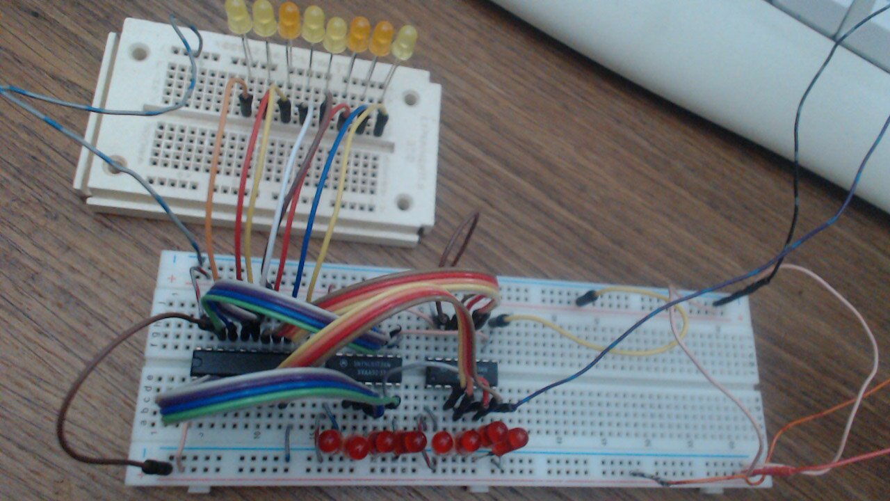
This initial breadboard layout follows Ben’s design but with the addition of a second smaller breadboard to display the contents of the data bus. It’s performance would be best described as haphazard, requiring much wiggling of cables to ensure they had a good breadboard connection. This was one of the reasons why I wanted to commit the design to a soldered circuit board but I was hoping to first gain some confidence that the design was ok.
Using fly cables from a TTL logic source I set a pattern of bits on the data bus which could then be loaded into the register. The bus was then cleared, disconnected from the logic source and that original bit pattern could be output from the register and onto the bus display. This input and output from the register proved it worked, just.
I’ll add a quick word on the three chip design because single TTL chip registers are available. The problem with those is that you can’t see what values the register is holding, whereas this design includes 2 x 4-bit flip-flops (74LS173’s to hold the register’s value) and a single 8-bit bus transceiver (74LS245 for input/output to the data bus). Rather than have these modules within a single chip this design offers the opportunity to place LEDs between the flip-flops and the transceiver to display register content.
Schematic for Three Registers:
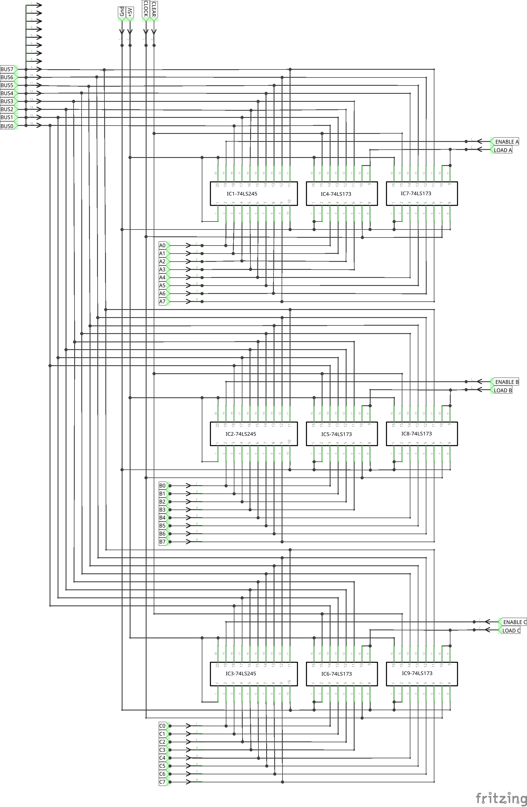
Here I have repeated the initial breadboard layout to provide three registers (A, B and C) on a single circuit. Each register has its own controls to output to the data bus (Enable) and to read from the data bus (Load). These controls are triggered by taking their voltage low (0v), otherwise they should be kept high (3-5v) to keep them inactive.
Common across all three registers is the power supply (+5v and Gnd), the 8 lines of the data bus, the Clock signal and a Clear flag. So Clear will initialize all three registers to zero. I considered seperate Clear flags for each register but opted for the simplicity of a single common clear command, probably only to be used at computer start-up.
Register contents can be measured from points A0-A7, B0-B7 and C0-C7. I haven’t hard-wired LEDs into the circuit but instead provided some output header pins.
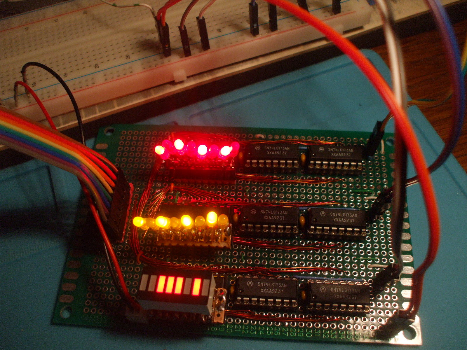
Blinkenlights:
One of the primary objectives of this project is to provide an insight into CPU operation. So LEDs at every opportunity would seem to be the order of the day. Yet I was beginning to doubt whether so many LEDs would affect CPU performance and, at higher speeds, whether they would be of any diagnostic help. I therefore decided to provide a row of 9 header pins at every opportunity (8 data bits + Gnd) to allow for the addition of LEDs (at low speeds), the connection of a logic analyser (at higher speeds), maybe cables to a control panel (one day) or simply nothing if everything was working ok. This led me to design several LED plug-in display modules.
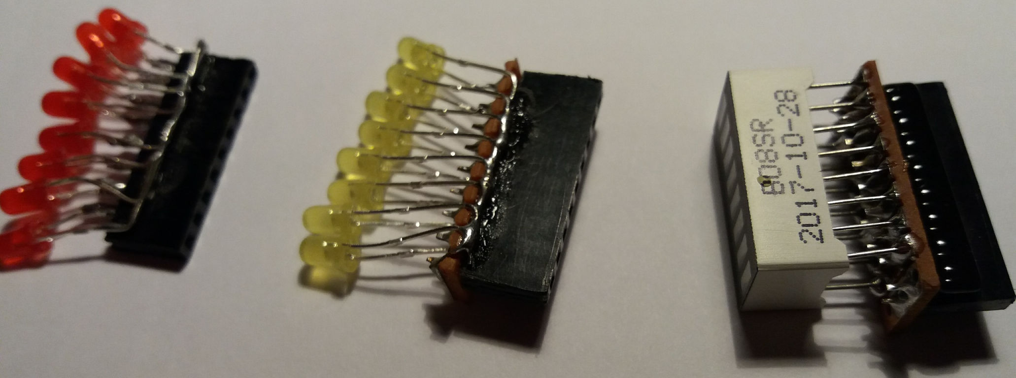
From left to right: a) the first was a combination of a 9-pin header and 8 x 3mm red LEDs with common cathodes connected to the 9th pin (Gnd), b) a similar arrangement with yellow LEDs but this time with a small 9×2 piece of stripboard which made it more robust when plugging in and out of boards, and finally c) an 8 segment bar graph module in a 16 pin package soldered to a 9×4 piece of stripboard, under which is a 9-pin header socket and a 9 pin resistor array with a common connection to the Gnd pin. c) was the most fiddly header to make (34 soldered connections on a 2.5x1cm board) but it proved to be the most robust and was the only one to offer resistor protection to its LEDs. Such protection isn’t necessary in this register module (as all LEDs are driven from TTL outputs) but I shall certainly make more of these as this TTL CPU evolves.
Update: I’ve since posted some notes to show how these 8-bit BlinkenLights Plug-ins are made.
Circuit board:
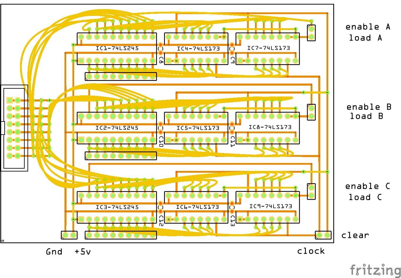
And here is the circuit schematic transferred to a circuit board design. Darker orange lines indicate under-board connections whilst the lighter yellow lines show the top layer connections. I’ve placed the 9-pin headers for the blinkenlights alongside each 74LS245 chip and moved Power, Clock and Clear connections to the bottom of the board.
The data bus connection will be via an IDC ribbon cable header on the left of the board. I considered several options for carrying 8-bit buses between boards and was keen on using CAT5 cable and RJ45 sockets at one point but couldn’t find any to fit my 2.54mm pitch boards. Ribbon cable is the orthodox choice but note that I’ll use 16-wire ribbon cable instead of 8. These present as a double row of 8 connectors which I’ll solder into pairs to provide an 8-way bus. This is neater than fanning-out 2 rows of 4 pins from an 8-wire ribbon cable and it also means I could solder many in parallel to provide multiple bus connections from a central hub.
Between all of the ICs I have added 100nF capacitors (C8 to C13). These were not on the schematic and they play no part in the logic of the circuit but they do help to prevent distortion on the power lines, which could affect performance. They hold a small charge which is quickly provided to the chips when they change state (i.e. signal transition from 0 -> 1). Without them the chips would rely on the power source and if that were slower to react then the expected square on/off data signals would start to become rounded and distorted, leading to errors as speeds increased. At this stage I’m not sure how much they will improve performance and whether I’ve got the ratio of capacitors to chips right but it is good practice to include them wherever you can.
Construction and Testing:
To hold three registers on the same board I have used an 8cm x 12cm double-sided perfboard which provides a 29 x 41 grid of holes. The order of construction was to solder the power lines to each IC socket, then the control lines (Clock, Clear, Load and Enable) and finally the data bus lines. At regular intervals I used the continuity feature of a multimeter to check all connections were as expected, doing this before the IC’s were inserted into their sockets.
Wiring convention on this board (I really should be consistent on every board but I tend to use whatever wires are available) were: +5v (red), Gnd (bare tinned wire), Clock (orange), Clear (white), Load (blue) and Enable (green). For the data lines I wanted something finer (that would pass through the 1mm circuit board holes) and opted to use enameled copper wire salvaged from an old transformer. This provided both red and clear enameled wire so I alternated their use, using one for even data lines and the other for odd numbered lines, hoping this would aid future fault finding. To solder these data bus wires I first used a craft knife to scrape the enamel from the end of each wire.
A minor design change to the initial circuit board layout is the addition of another 9-pin header, this time to enable display or testing of the 8 data bus lines – plus one connection to Gnd. In the above photo these data bus pin headers have been used to attach wires to provide a test signal onto the bus. The other 9-pin headers have my blinkenlights plug-ins to display the contents of each register.
To test the registers without having yet created the rest of this 8-bit CPU I connected a 1-second clock source to the Clock pin and used a breadboard to plug all other control and data pins into the 5v supply or Gnd to simulate TTL high and low signals respectively. Clear was kept low, if set high then the contents of all registers cleared (tick). All other control pins were kept high whilst different patterns of high’s and low’s were set on the data bus. Taking each Load pin temporarily low in turn would load the current data bus pattern into that register (tick). The data bus was then disconnected. Placing a registers Enable pin low would output that registers contents onto the data bus (tick). If another register’s Load pin was taken low at the same time then that register would load the new contents of the data bus (tick). Thus by manipulating these control pins I could transfer the contents of any register to one of the other registers (big tick). Finally, to check for any loose connections I gently pressed each chip during operation to ensure there was no flickering of LEDs or unexpected results.
Now I don’t want to give the impression that everything tested ok and worked first time. These things rarely do, so don’t be disheartened or discouraged when a build doesn’t go to plan. What’s important is that you remain calm and methodically check each possible cause of the fault. I had several poorly soldered connections which required re-heating and a drop more solder (my fault for being too stingey with the solder in the first place). When re-soldering such joints remember to pop the IC’s out of their sockets to protect them from the heat.
Parts List:

	80x120mm double-sided prototype PCB (a.k.a. perfboard)
	C8-13	Ceramic Capacitor 100nF
	IC1-3	74LS245 8-bit bus transceiver, non-inverting, tristate (i.e. on, off and disconnected)
	IC4-9	74LS173 4-bit flip-flop, tristate with asynchronous clear (i.e. a pin to clear contents)
	9 x		20 and 16-pin IC sockets for the above ICs
	1 x		JST PH 2-pin male connector (for power supply - I prefer a click & hold socket for these)
	4 x		2-pin male headers (for control lines)
	4 x		9-pin male headers (for connecting optional blinkenlights)
	1 x		16-pin (2 rows of 8) male IDC box header (for ribbon cable connection)
	and various bits of wire and enamel coated copper from scraps.
Most of the above were from odds and ends that I already had, but to give an indication of the massive financial outlay required for this project… the PCB was the most expensive item at £0.95 (approx. $1.34) and all the chips together cost £2.91 ($4.09). The main investment was the hours of breadboard prototyping, on-screen design and final construction in the hope that this would work!
That’s three general purpose registers completed for my “Hol-1” 8-bit CPU. Next the Arithmetic & Logic Unit (ALU).
Categorised as: Homebrew 8-Bit CPU
Comments are disabled on this post