8-Bit CPU – Clock —
Building a CPU clock and controller from 555 timers and TTL logic.
Update: Please note my later post which contains an improvement to this TTL clock signal generator.
Why?:
Back in 2015 when I posted an item on Logic Buffers I intended to produce follow-up posts covering common logic chips. Producing each in a simple resistor transistor logic (RTL) format. I was then going to move up a level and use transistor transistor logic (TTL) to produce more complex circuits, culminating in a computer’s central processing unit (CPU).
But hey, I don’t get enough spare time and my enthusiasm to reach that end goal project is getting the better of me. This enthusiasm has been spurred on by the book ‘Code’ by Charles Petzold (Microsoft Press). A cracking read that will leave any geek with a burning desire to design and build their own computer.
Not the sort of build that involves plugging CPU and memory chips into a motherboard but the sort that involves many individual TTL logic chips, lots of wires, your own machine language and lots and lots of ‘blinkenlights’.
After some research into the world of home-brewed 8-bit CPUs I came across a series of 41 fantastic videos by Ben Eater titled “Build an 8-bit computer from scratch”. Although keen to eventually design my own CPU, by initially following Ben’s design I will learn loads and have ideas for future improvements.
Although I’m not one to follow even Ben’s wise instructions to the letter. Not that I think I know better but I will need to substitute items to make best use of what’s available to me.
My first substitution will be soldered circuit boards rather than breadboards. I will use breadboards to build and test each module but I would prefer to then transfer them to perfboard or veroboard. Breadboards are great but mine never look as neat and tidy as Ben’s and I know my mess of spaghetti wiring will lead to temperamental problems. I also want to build something permanent. A version 1.0 that I can look back and laugh at when version 5.0 is (hopefully) so much better.

This initial breadboard layout includes a red led ‘power on’ indicator (top centre) and an orange clock led (bottom right) as well as the main green clock led (top right). I removed both (red & orange) from the final design as they didn’t provide any needed purpose.
Clock Source:
The computer needs a heartbeat to synchronise the operation of each module. So a basic square wave signal generator is the first step and this circuit provides two options using NE555 timer chips. This was a nostalgic trip back in time for me as my first book on electronics was the Radio Shack Engineer’s Mini-Notebook on 555’s bought from my local Tandy store in the 1970’s.
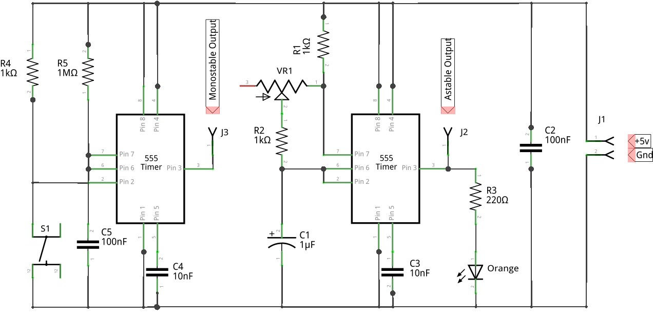
The first clock source option (centre right of schematic) uses a 555 in its astable mode to generate a signal of variable frequency via use of a potentiometer. Speed and timing precision isn’t important with this v1.0 computer so crystal oscillators and calibrated frequency counters are unnecessary. My version provides a clean square wave from 0.7Hz to 480Hz.
The second clock source option (left of schematic) uses another 555 in its monostable mode to generate a pulsed signal via use of a button. This will be an important function that will enable me to step through and debug machine code programs.
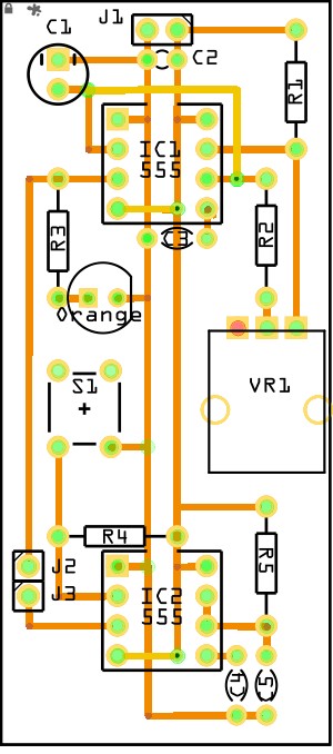
Having tested these circuits on a breadboard (left half of the first photo) I then combined the two clock source options onto a single 10×24 hole perfboard. I was tempted to mount the button, pot and LEDs onto a control panel but decided to keep these clock sources as a single board that could be replaced or re-used as necessary.
Another variance from the original design is an orange LED on the astable output. Prior to switching from ‘manual’ monostable to ‘automated’ astable mode this will be helpful to show how fast astable is running.
Parts List:
C1		Electrolytic Capacitor  1µF
C2,5	Ceramic Capacitor  100nF
C3,4	Ceramic Capacitor  10nF
IC1,2	555 Timer
J1		[Gnd, +5v] power lines
J2		Astable (variable pulse) output
J3		Monostable (button step) output
Orange	LED
R1,2,4	1kΩ Resistor
R5		1MΩ Resistor
S1		Pushbutton
VR1		1MΩ
Thinking ahead for future versions I may look to increase C5. This would slow the pace of manually stepping through programs with the button and removes the risk of stepping too fast and missing the code I wanted to examine. Or, if possible, debug watch points could be added to programs to trigger a halt. I may then be able to switch to manual stepping, free the halt and continue?
Clock Select:
Now I have a couple of clock signal sources I need a means of switching between them. Such switching needs to be smooth and not jittery or there’ll be a risk of spurious pulse signals that would cause the computer to step past the code I need to debug. This ‘de-bouncing’ of the switch is performed by another 555 chip but this time wired in a bistable mode.
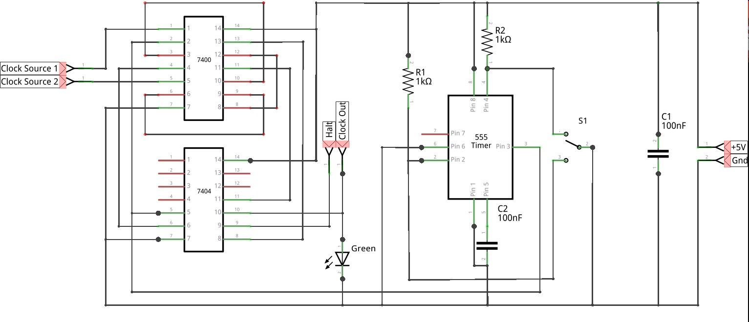
Some TTL logic chips are then used to take the output from this de-bounced switch to toggle between the two clock sources and therefore provide a single clock signal for the computer. This logic is further complicated by the provision of a halt input that can be used to disable the clock and therefore halt the computer. Such a halt could be achieved by me switching the clock source to manual but this halt input isn’t intended for me to use but for the computer so that it can stop itself at the end of a program.
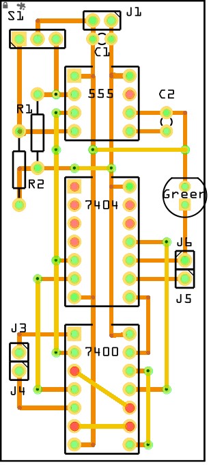
I’ve combined all this clock select circuitry onto a second 10×24 hole perfboard, the second interchangeable module for this computer. Keeping clock select separate from the clock source circuit board means I can plug in alternate clock sources e.g. from a signal generator running at higher speeds to identify the upper speed limit of this computer design.
In a variance from the original design I’ve replaced the three logic chips (74LS04, 74LS08, 74LS32) with two chips (74LS00, 74LS04). This logic simplification from 3xAND gates, 2xNOTs and 1xOR to 4xNANDs and 3xNOTs was necessary to fit onto the small perfboard and utilise available chips.
Parts List:
555		Timer
7400	Quad 2-input NAND gate
7404	Hex inverter
C1,2	Ceramic Capacitor  100nF
Green	LED
J1		[Gnd, +5v] power lines
J3,4	clock signal inputs
J5		Halt input
J6		Selected clock output signal
R1,2	1kΩ Resistor
S1		Toggle Switch
For future versions of my own design I would like to experiment with crystal oscillators and maybe incorporate a frequency counter? For this version I want the circuit boards to be on display but for future versions I would probably encase the boards and run leads to a control panel for buttons, LEDs, etc… With this in mind these two small boards are stackable (with clock select to go on top) with power and clock connections aligned to make best use of any enclosure space.
Construction:
That’s a completed clock module or rather a clock source and a clock select module. For a thorough explanation of how they work then please visit Ben Eater’s website and follow his great videos.
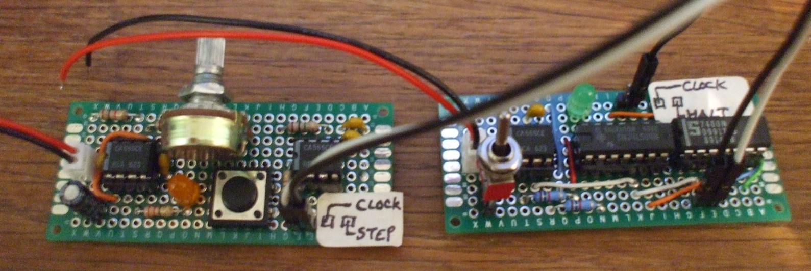
Here clock-source is on the left and clock-select on the right. The potentiometer on clock-source is a little over-sized (best I had) and the toggle switch on clock-select needed to be soldered to header pins to attach it to the board. I’ll replace that toggle switch when I find a latching push button ‘tactile switch’ that fits the 2.54mm board pitch.
Despite costing more than some of the chips used I decided to use IC sockets throughout. They remove the risk of damaging chips during soldering and, should I scrap a design, they make the chips easy to recover.
For board to board connections I’ve opted for male headers on the boards and will use female to female cables.
For power connections I’ve used some JST clip connectors that I had available. They’re a pain to unclip (using tweezers) but secure when clipped in. In my final layout I’ll have to create a power wiring loom to connect these to. In the meantime they plug into a breadboard power rail.
On board jumper wires are generally 26AWG solid core wire (preferred as they pass through the perfboard holes) and I’ll use as many colours as I can find to aid tracing wires when fault-finding.
The Clock-select pcb design shows a couple of pin to pin connections under the 7400 that cross the power rails. When it came to construction I looped these around the IC instead. It just felt like the better thing to do.
There are a few pins left unconnected on the 7404 which I probably should connect to Vcc or Gnd to reduce power consumption but I’m not currently sure which is best.
I’ve used Fritzing software for the circuit schematics and the PCB designs.
That’s my 8-bit CPU clock modules completed, which I’ll tag as “Hol-1”. Next the registers.
Categorised as: Homebrew 8-Bit CPU
Comments are disabled on this post